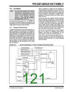
PIC24FJ64GA104 FAMILY
10.4.3
CONTROLLING PERIPHERAL PIN
SELECT
10.4.3.1
Input Mapping
The inputs of the Peripheral Pin Select options are
mapped on the basis of the peripheral; that is, a control
register associated with a peripheral dictates the pin it
will be mapped to. The RPINRx registers are used to
configure peripheral input mapping (see Register 10-1
through Register 10-14). Each register contains up to
two sets of 5-bit fields, with each set associated with
one of the pin-selectable peripherals. Programming a
given peripheral’s bit field with an appropriate 6-bit
value maps the RPn pin with that value to that
peripheral. For any given device, the valid range of
values for any of the bit fields corresponds to the
maximum number of Peripheral Pin Select options
supported by the device.
Peripheral Pin Select features are controlled through
two sets of Special Function Registers: one to map
peripheral inputs and one to map outputs. Because
they are separately controlled, a particular peripheral’s
input and output (if the peripheral has both) can be
placed on any selectable function pin without
constraint.
The
association
of
a
peripheral
to
a
peripheral-selectable pin is handled in two different
ways, depending on if an input or an output is being
mapped.
TABLE 10-2: SELECTABLE INPUT SOURCES (MAPS INPUT TO FUNCTION)(1)
Function Mapping
Bits
Input Name
Function Name
Register
External Interrupt 1
External Interrupt 2
Input Capture 1
INT1
INT2
RPINR0
RPINR1
RPINR7
RPINR7
RPINR8
RPINR8
RPINR9
RPINR11
RPINR11
RPINR20
RPINR20
RPINR21
RPINR22
RPINR22
RPINR23
RPINR3
RPINR3
RPINR4
RPINR4
RPINR18
RPINR18
RPINR19
RPINR19
INT1R<5:0>
INT2R<5:0>
IC1R<5:0>
IC1
Input Capture 2
IC2
IC2R<5:0>
Input Capture 3
IC3
IC3R<5:0>
Input Capture 4
IC4
IC4R<5:0>
Input Capture 5
IC5
IC5R<5:0>
Output Compare Fault A
Output Compare Fault B
SPI1 Clock Input
OCFA
OCFB
SCK1IN
SDI1
OCFAR<5:0>
OCFBR<5:0>
SCK1R<5:0>
SDI1R<5:0>
SS1R<5:0>
SCK2R<5:0>
SDI2R<5:0>
SS2R<5:0>
T2CKR<5:0>
T3CKR<5:0>
T4CKR<5:0>
T5CKR<5:0>
U1CTSR<5:0>
U1RXR<5:0>
U2CTSR<5:0>
U2RXR<5:0>
SPI1 Data Input
SPI1 Slave Select Input
SPI2 Clock Input
SS1IN
SCK2IN
SDI2
SPI2 Data Input
SPI2 Slave Select Input
Timer2 External Clock
Timer3 External Clock
Timer4 External Clock
Timer5 External Clock
UART1 Clear To Send
UART1 Receive
SS2IN
T2CK
T3CK
T4CK
T5CK
U1CTS
U1RX
U2CTS
U2RX
UART2 Clear To Send
UART2 Receive
Note 1: Unless otherwise noted, all inputs use the Schmitt Trigger input buffers.
DS39951C-page 124
2010 Microchip Technology Inc.

 MICROCHIP [ MICROCHIP ]