PIC24FJ64GA104 FAMILY
10.1.1
OPEN-DRAIN CONFIGURATION
10.2.2
ANALOG INPUT PINS AND
VOLTAGE CONSIDERATIONS
In addition to the PORT, LAT and TRIS registers for
data control, each port pin can also be individually
configured for either digital or open-drain output. This is
controlled by the Open-Drain Control register, ODCx,
associated with each port. Setting any of the bits con-
figures the corresponding pin to act as an open-drain
output.
The voltage tolerance of pins used as device inputs is
dependent on the pin’s input function. Pins that are
used as digital only inputs are able to handle DC
voltages up to 5.5V, a level typical for digital logic
circuits. In contrast, pins that also have analog input
functions of any kind can only tolerate voltages up to
VDD. Voltage excursions beyond VDD on these pins
should be avoided.
The open-drain feature allows the generation of
outputs higher than VDD (e.g., 5V) on any desired
digital only pins by using external pull-up resistors. The
maximum open-drain voltage allowed is the same as
the maximum VIH specification.
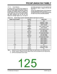
Table 10-1 summarizes the input voltage capabilities.
Refer to Section 28.0 “Electrical Characteristics” for
more details.
10.2 Configuring Analog Port Pins
TABLE 10-1: INPUT VOLTAGE TOLERANCE
Tolerated
The AD1PCFGL and TRIS registers control the opera-
tion of the A/D port pins. Setting a port pin as an analog
input also requires that the corresponding TRIS bit be
set. If the TRIS bit is cleared (output), the digital output
level (VOH or VOL) will be converted.
Port or Pin
Description
Input
PORTA<4:0>
VDD
Only VDD input levels
tolerated.
PORTB<15:12>
PORTB<4:0>
When reading the PORT register, all pins configured as
analog input channels will read as cleared (a low level).
PORTC<3:0>(1)
PORTA<10:7>(1)
PORTB<11:7>
PORTB<6:5>
5.5V
Tolerates input levels
above VDD, useful for
most standard logic.
Pins configured as digital inputs will not convert an
analog input. Analog levels on any pin that is defined as
a digital input (including the ANx pins) may cause the
input buffer to consume current that exceeds the
device specifications.
PORTC<9:4>(1)
Note 1: Not available on 28-pin devices.
10.2.1
I/O PORT WRITE/READ TIMING
One instruction cycle is required between a port
direction change or port write operation and a read
operation of the same port. Typically, this instruction
would be a NOP(Example 10-1).
EXAMPLE 10-1:
PORT WRITE/READ EXAMPLE
MOV
MOV
NOP
0xFF00, W0
W0, TRISB
; Configure PORTB<15:8> as inputs
; and PORTB<7:0> as outputs
; Delay 1 cycle
BTSS PORTB, #13
; Next Instruction
DS39951C-page 122
2010 Microchip Technology Inc.

 MICROCHIP [ MICROCHIP ]