PIC18CXX2
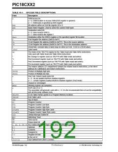
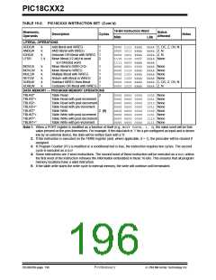
TABLE 19-1: OPCODE FIELD DESCRIPTIONS
Field
Description
a
RAM access bit
a = 0: RAM location in Access RAM (BSR register is ignored)
a = 1: RAM bank is specified by BSR register
bbb
BSR
d
Bit address within an 8-bit file register (0 to 7)
Bank Select Register. Used to select the current RAM bank.
Destination select bit;
d = 0: store result in WREG,
d = 1: store result in file register f.
dest
f
Destination either the WREG register or the specified register file location
8-bit Register file address (0x00 to 0xFF)
fs
12-bit Register file address (0x000 to 0xFFF). This is the source address.
12-bit Register file address (0x000 to 0xFFF). This is the destination address.
Literal field, constant data or label (may be either an 8-bit, 12-bit or a 20-bit value)
Label name
fd
k
label
mm
The mode of the TBLPTR register for the Table Read and Table Write instructions
Only used with Table Read and Table Write instructions:
*
No Change to register (such as TBLPTR with Table reads and writes)
Post-Increment register (such as TBLPTR with Table reads and writes)
Post-Decrement register (such as TBLPTR with Table reads and writes)
Pre-Increment register (such as TBLPTR with Table reads and writes)
*+
*-
+*
n
The relative address (2’s complement number) for relative branch instructions, or the direct
address for Call/Branch and Return instructions
PRODH
PRODL
s
Product of Multiply high byte
Product of Multiply low byte
Fast Call / Return mode select bit.
s = 0: do not update into/from shadow registers
s = 1: certain registers loaded into/from shadow registers (Fast mode)
u
Unused or Unchanged
WREG
x
Working register (accumulator)
Don't care (0 or 1)
The assembler will generate code with x = 0. It is the recommended form of use for compatibility
with all Microchip software tools.
TBLPTR
TABLAT
TOS
21-bit Table Pointer (points to a Program Memory location)
8-bit Table Latch
Top of Stack
PC
Program Counter
PCL
Program Counter Low Byte
Program Counter High Byte
Program Counter High Byte Latch
Program Counter Upper Byte Latch
Global Interrupt Enable bit
Watchdog Timer
PCH
PCLATH
PCLATU
GIE
WDT
TO
Time-out bit
PD
Power-down bit
C, DC, Z, OV, N ALU status bits Carry, Digit Carry, Zero, Overflow, Negative
[ ]
( )
→
Optional
Contents
Assigned to
< >
Register bit field
In the set of
italics
User defined term (font is courier)
DS39026B-page 192
Preliminary
7/99 Microchip Technology Inc.

 MICROCHIP [ MICROCHIP ]