PIC18CXX2
The control instructions may use some of the following
operands:
19.0 INSTRUCTION SET SUMMARY
The PIC18CXXX instruction set adds many enhance-
ments to the previous PICmicro instruction sets, while
maintaining an easy migration from these PICmicro
instruction sets.
• A program memory address (specified by the
value of ’n’)
• The mode of the Call or Return instructions (spec-
ified by the value of ’s’)
• The mode of the Table Read and Table Write
instructions (specified by the value of ’m’)
• No operand required
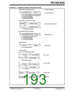
Most instructions are a single program memory word
(16-bits), but there are three instructions that require
two program memory locations.
Each single word instruction is a 16-bit word divided
into an OPCODE, which specifies the instruction type
and one or more operands, which further specify the
operation of the instruction.
(specified by the value of ’—’)
All instructions are a single word, except for three dou-
ble word instructions. These three instructions were
made double word instructions so that all the required
information is available in these 32-bits. In the second
word, the 4-MSb’s are 1’s. If this second word is exe-
cuted as an instruction (by itself), it will execute as a
NOP.
The instruction set is highly orthogonal and is grouped
into four basic categories:
• Byte-oriented operations
• Bit-oriented operations
• Literal operations
All single word instructions are executed in a single
instruction cycle, unless a conditional test is true or the
program counter is changed as a result of the instruc-
tion. In these cases, the execution takes two instruction
cycles with the additional instruction cycle(s) executed
as a NOP.
• Control operations
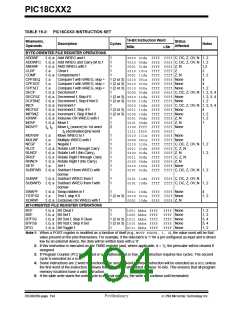
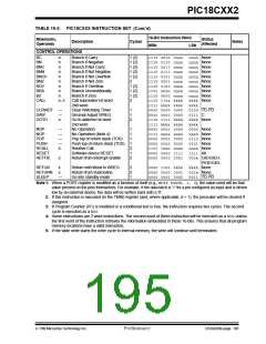
The PIC18CXXX instruction set summary in
Table 19-2 lists byte-oriented, bit-oriented, literal
and control operations. Table 19-1 shows the
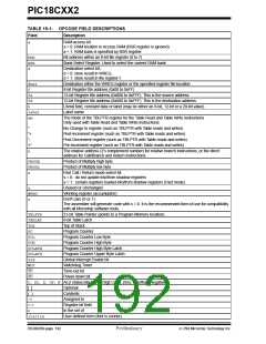
opcode field descriptions.
The double word instructions execute in two instruction
cycles.
Most byte-oriented instructions have three operands:
1. The file register (specified by the value of ’f’)
One instruction cycle consists of four oscillator periods.
Thus, for an oscillator frequency of 4 MHz, the normal
instruction execution time is 1 µs. If a conditional test is
true or the program counter is changed as a result of an
instruction, the instruction execution time is 2 µs. Two
word branch instructions (if true) would take 3 µs.
2. The destination of the result
(specified by the value of ’d’)
3. The accessed memory
(specified by the value of ’a’)
'f' represents a file register designator and 'd' repre-
sents a destination designator. The file register desig-
nator specifies which file register is to be used by the
instruction.
Figure 19-1 shows the general formats that the instruc-
tions can have.
All examples use the following format to represent a
hexadecimal number:
The destination designator specifies where the result of
the operation is to be placed. If 'd' is zero, the result is
placed in the WREG register. If 'd' is one, the result is
placed in the file register specified in the instruction.
0xhh
where h signifies a hexadecimal digit.
All bit-oriented instructions have three operands:
The Instruction Set Summary, shown in Table 19-2,
lists the instructions recognized by the Microchip
assembler (MPASM).
1. The file register (specified by the value of ’f’)
2. The bit in the file register
(specified by the value of ’b’)
Section 19.1 provides a description of each instruction.
3. The accessed memory
(specified by the value of ’a’)
'b' represents a bit field designator which selects the
number of the bit affected by the operation, while 'f' rep-
resents the number of the file in which the bit is located.
The literal instructions may use some of the following
operands:
• A literal value to be loaded into a file register
(specified by the value of ’k’)
• The desired FSR register to load the literal value
into (specified by the value of ’f’)
• No operand required
(specified by the value of ’—’)
7/99 Microchip Technology Inc.
Preliminary
DS39026B-page 191

 MICROCHIP [ MICROCHIP ]