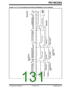
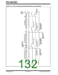
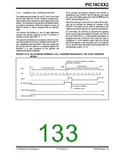
PIC18CXX2
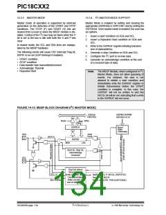
14.3.4.1 I2C MASTER MODE OPERATION
A typical transmit sequence would go as follows:
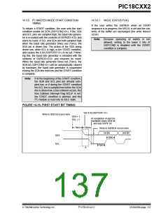
a) The user generates a Start Condition by setting
the START enable bit SEN (SSPCON2<0>).
The master device generates all of the serial clock
pulses and the START and STOP conditions. A trans-
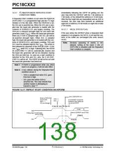
fer is ended with a STOP condition or with a repeated
START condition. Since the repeated START condition
is also the beginning of the next serial transfer, the I2C
bus will not be released.
b) SSPIF is set. The MSSP module will wait the
required start time before any other operation
takes place.
c) The user loads the SSPBUF with the address to
transmit.
In Master transmitter mode serial data is output through
SDA, while SCL outputs the serial clock. The first byte
transmitted contains the slave address of the receiving
device (7 bits) and the Read/Write (R/W) bit. In this
case, the R/W bit will be logic ’0’. Serial data is trans-
mitted 8 bits at a time. After each byte is transmitted, an
acknowledge bit is received. START and STOP condi-
tions are output to indicate the beginning and the end
of a serial transfer.
d) Address is shifted out the SDA pin until all 8 bits
are transmitted.
e) The MSSP Module shifts in the ACK bit from the
slave device and writes its value into the
SSPCON2 register (SSPCON2<6>).
f) The MSSP module generates an interrupt at the
end of the ninth clock cycle by setting the SSPIF
bit.
In Master receive mode, the first byte transmitted con-
tains the slave address of the transmitting device
(7 bits) and the R/W bit. In this case, the R/W bit will be
logic ’1’. Thus, the first byte transmitted is a 7-bit slave
address followed by a ’1’ to indicate receive bit. Serial
data is received via SDA, while SCL outputs the serial
clock. Serial data is received 8 bits at a time. After each
byte is received, an acknowledge bit is transmitted.
START and STOP conditions indicate the beginning
and end of transmission.
g) The user loads the SSPBUF with eight bits of
data.
h) DATA is shifted out the SDA pin until all 8 bits are
transmitted.
i) The MSSP Module shifts in the ACK bit from the
slave device and writes its value into the
SSPCON2 register (SSPCON2<6>).
j) The MSSP module generates an interrupt at the
end of the ninth clock cycle by setting the SSPIF
bit.
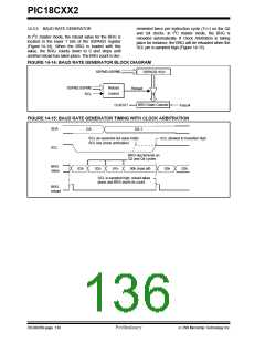
The baud rate generator used for the SPI mode opera-
tion is now used to set the SCL clock frequency for
either 100 kHz, 400 kHz or 1 MHz I2C operation. The
baud rate generator reload value is contained in the
lower 7 bits of the SSPADD register. The baud rate gen-
erator will automatically begin counting on a write to the
SSPBUF. Once the given operation is complete, (i.e.
transmission of the last data bit is followed by ACK), the
internal clock will automatically stop counting and the
SCL pin will remain in its last state.
k) The user generates a STOP condition by setting
the STOP enable bit PEN (SSPCON2<2>).
l) Interrupt is generated once the stop condition is
complete.
7/99 Microchip Technology Inc.
Preliminary
DS39026B-page 135

 MICROCHIP [ MICROCHIP ]