PIC18CXX2
The SSPCON1 register allows control of the I2C oper-
ation. Four mode selection bits (SSPCON<3:0>) allow
one of the following I2C modes to be selected:
• I2C Master mode, clock = OSC/4 (SSPADD +1)
• I2C Slave mode (7-bit address)
• I2C Slave mode (10-bit address)
SSPBUF register.
b) The buffer full bit BF is set.
c) An ACK pulse is generated.
d) MSSP interrupt flag bit SSPIF (PIR1<3>) is set
(interrupt is generated if enabled) on the falling
edge of the ninth SCL pulse.
• I2C Slave mode (7-bit address), with start and
stop bit interrupts enabled
• I2C Slave mode (10-bit address), with start and
stop bit interrupts enabled
• I2C Firmware controlled master operation, slave
is idle
Selection of any I2C mode, with the SSPEN bit set,
forces the SCL and SDA pins to be open drain, pro-
vided these pins are programmed to inputs by setting
the appropriate TRISC bits.
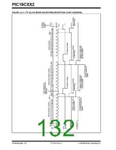
In 10-bit address mode, two address bytes need to be
received by the slave. The five Most Significant bits
(MSbs) of the first address byte specify if this is a 10-bit
address. Bit R/W (SSPSTAT<2>) must specify a write
so the slave device will receive the second address
byte. For a 10-bit address, the first byte would equal
‘1111 0 A9 A8 0’, where A9 and A8 are the two MSbs
of the address. The sequence of events for 10-bit
address is as follows with steps 7- 9 for slave-transmit-
ter:
1. Receive first (high) byte of Address (bits SSPIF,
BF and bit UA (SSPSTAT<1>) are set).
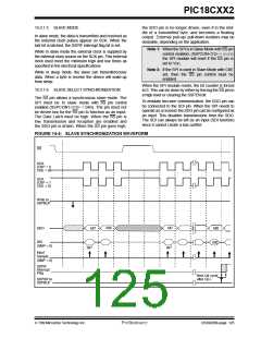
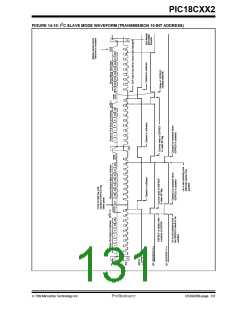
14.3.1 SLAVE MODE
2. Update the SSPADD register with second (low)
byte of Address (clears bit UA and releases the
SCL line).
In slave mode, the SCL and SDA pins must be config-
ured as inputs (TRISC<4:3> set). The MSSP module
will override the input state with the output data when
required (slave-transmitter).
3. Read the SSPBUF register (clears bit BF) and
clear flag bit SSPIF.
When an address is matched or the data transfer after
an address match is received, the hardware automati-
cally will generate the acknowledge (ACK) pulse and
load the SSPBUF register with the received value cur-
rently in the SSPSR register.
4. Receive second (low) byte of Address (bits
SSPIF, BF, and UA are set).
5. Update the SSPADD register with the first (high)
byte of Address. If match releases SCL line, this
will clear bit UA.
There are certain conditions that will cause the MSSP
module not to give this ACK pulse. These are if either
(or both):
6. Read the SSPBUF register (clears bit BF) and
clear flag bit SSPIF.
7. Receive repeated START condition.
a) The buffer full bit BF (SSPSTAT<0>) was set
before the transfer was received.
8. Receive first (high) byte of Address (bits SSPIF
and BF are set).
b) The overflow bit SSPOV (SSPCON<6>) was set
before the transfer was received.
9. Read the SSPBUF register (clears bit BF) and
clear flag bit SSPIF.
In this case, the SSPSR register value is not loaded
into the SSPBUF, but bit SSPIF (PIR1<3>) is set. The
BF bit is cleared by reading the SSPBUF register, while
bit SSPOV is cleared through software.
The SCL clock input must have a minimum high and
low for proper operation. The high and low times of the
I2C specification, as well as the requirement of the
MSSP module, is shown in timing parameter #100 and
parameter #101.
14.3.1.1 ADDRESSING
Once the MSSP module has been enabled, it waits for
a START condition to occur. Following the START con-
dition, the 8-bits are shifted into the SSPSR register. All
incoming bits are sampled with the rising edge of the
clock (SCL) line. The value of register SSPSR<7:1> is
compared to the value of the SSPADD register. The
address is compared on the falling edge of the eighth
clock (SCL) pulse. If the addresses match, and the BF
and SSPOV bits are clear, the following events occur:
a) The SSPSR register value is loaded into the
7/99 Microchip Technology Inc.
Preliminary
DS39026B-page 129

 MICROCHIP [ MICROCHIP ]