PIC18F6525/6621/8525/8621
the holding registers are written. At the end of updating
8 registers, the EECON1 register must be written to, to
start the programming operation with a long write.
5.5
Writing to Flash Program Memory
The minimum programming block is 4 words or 8 bytes.
Word or byte programming is not supported.
The long write is necessary for programming the
internal Flash. Instruction execution is halted while in a
long write cycle. The long write will be terminated by
the internal programming timer.
Table writes are used internally to load the holding
registers needed to program the Flash memory. There
are 8 holding registers used by the table writes for
programming.
The EEPROM on-chip timer controls the write time.
The write/erase voltages are generated by an on-chip
charge pump, rated to operate over the voltage range
of the device for byte or word operations.
Since the Table Latch (TABLAT) is only a single byte,
the TBLWT instruction has to be executed 8 times for
each programming operation. All of the table write
operations will essentially be short writes because only
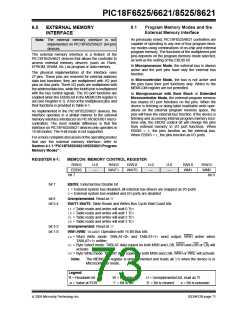
FIGURE 5-5:
TABLE WRITES TO FLASH PROGRAM MEMORY
TABLAT
Write Register
8
8
8
8
TBLPTR = xxxxx0
TBLPTR = xxxxx2
TBLPTR = xxxxx7
Holding Register
TBLPTR = xxxxx1
Holding Register
Holding Register
Holding Register
Program Memory
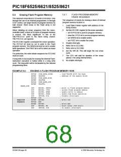
8. Disable interrupts.
5.5.1
FLASH PROGRAM MEMORY WRITE
SEQUENCE
9. Write 55h to EECON2.
10. Write AAh to EECON2.
The sequence of events for programming an internal
program memory location should be:
11. Set the WR bit. This will begin the write cycle.
12. The CPU will stall for duration of the write (about
2 ms using internal timer).
1. Read 64 bytes into RAM.
2. Update data values in RAM as necessary.
13. Re-enable interrupts.
3. Load Table Pointer register with address being
erased.
14. Repeat steps 6-14 seven times to write 64 bytes.
15. Verify the memory (table read).
4. Do the row erase procedure.
5. Load Table Pointer register with address of first
byte being written.
This procedure will require about 18 ms to update one
row of 64 bytes of memory. An example of the required
code is given in Example 5-3.
6. Write the first 8 bytes into the holding registers
with auto-increment.
Note:
Before setting the WR bit, the Table
Pointer address needs to be within the
intended address range of the eight bytes
in the holding register.
7. Set the EECON1 register for the write operation:
• set EEPGD bit to point to program memory;
• clear the CFGS bit to access program memory;
• set WREN to enable byte writes.
2005 Microchip Technology Inc.
DS39612B-page 67

 MICROCHIP [ MICROCHIP ]