PIC18F6525/6621/8525/8621
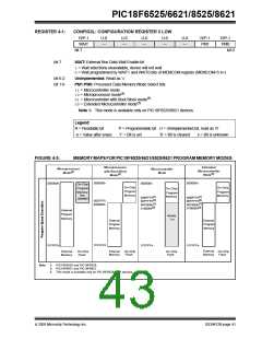
REGISTER 4-1:
CONFIG3L: CONFIGURATION REGISTER 3 LOW
R/P-1
WAIT
U-0
—
U-0
—
U-0
—
U-0
—
U-0
—
R/P-1
PM1
R/P-1
PM0
bit 7
bit 0
bit 7
WAIT: External Bus Data Wait Enable bit
1= Wait selections unavailable, device will not wait
0= Wait programmed by WAIT1 and WAIT0 bits of MEMCOM register (MEMCOM<5:4>)
bit 6-2
bit 1-0
Unimplemented: Read as ‘0’
PM1:PM0: Processor Data Memory Mode Select bits
11= Microcontroller mode
10= Microprocessor mode(1)
01= Microcontroller with Boot Block mode(1)
00= Extended Microcontroller mode(1)
Note 1: This mode is available only on PIC18F8525/8621 devices.
Legend:
R = Readable bit
P = Programmable bit U = Unimplemented bit, read as ‘0’
‘1’ = Bit is set ‘0’ = Bit is cleared x = Bit is unknown
-n = Value after erase
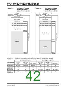
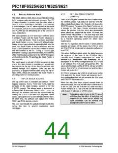
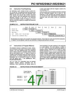
FIGURE 4-3:
MEMORY MAPS FOR PIC18F6525/6621/8525/8621 PROGRAM MEMORY MODES
Microprocessor
with Boot Block
Mode(3)
Extended
Microcontroller
Mode(3)
Microprocessor
Microcontroller
Mode
Mode(3)
000000h
000000h
000000h
000000h
On-Chip
Program
Memory
(No
On-Chip
On-Chip
On-Chip
Program
Memory
Program
Memory
Program
Memory
00BFFFh(1)
00FFFFh(2)
00C000h(1)
010000h(2)
00BFFFh(1)
00FFFFh(2)
00C000h(1)
010000h(2)
access)
0007FFh
000800h
External
Program
Memory
Reads
‘0’s
External
Program
Memory
External
Program
Memory
1FFFFFh
1FFFFFh
1FFFFFh
1FFFFFh
External
Memory
External On-Chip
Memory Flash
External
Memory
On-Chip
Flash
On-Chip
Flash
On-Chip
Flash
Note 1: PIC18F8525 and PIC18F6525.
2: PIC18F8621 and PIC18F6621.
3: This mode is available only on PIC18F8525/8621 devices.
2005 Microchip Technology Inc.
DS39612B-page 41

 MICROCHIP [ MICROCHIP ]