PIC17C75X
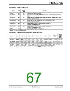
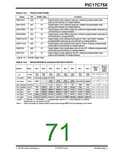
TABLE 10-3: PORTB FUNCTIONS
Name
Bit
Buffer Type
Function
RB0/CAP1
bit0
ST
Input/Output or the Capture1 input pin. Software programmable weak
pull-up and interrupt on change features.
RB1/CAP2
RB2/PWM1
RB3/PWM2
RB4/TCLK12
RB5/TCLK3
RB6/SCK
bit1
bit2
bit3
bit4
bit5
bit6
bit7
ST
ST
ST
ST
ST
ST
ST
Input/Output or the Capture2 input pin. Software programmable weak
pull-up and interrupt on change features.
Input/Output or the PWM1 output pin. Software programmable weak pull-up
and interrupt on change features.
Input/Output or the PWM2 output pin. Software programmable weak pull-up
and interrupt on change features.
Input/Output or the external clock input to Timer1 and Timer2. Software
programmable weak pull-up and interrupt on change features.
Input/Output or the external clock input to Timer3. Software programmable
weak pull-up and interrupt on change features.
Input/Output or the master/slave clock for the SPI. Software programmable
weak pull-up and interrupt on change features.
RB7/SDO
Input/Output or data output for the SPI. Software programmable weak
pull-up and interrupt on change features.
Legend: ST = Schmitt Trigger input.
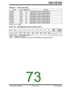
TABLE 10-4: REGISTERS/BITS ASSOCIATED WITH PORTB
Value on
all other
resets
Value on
POR,
BOR
Address
Name
Bit 7
Bit 6
Bit 5
Bit 4
Bit 3
Bit 2
Bit 1
Bit 0
(Note1)
RB7/
SDO
RB6/
SCK
RB5/
TCLK3
RB4/
TCLK12
RB3/
PWM2
RB2/
PWM1
RB1/
CAP2
RB0/
CAP1
xxxx xxxx uuuu uuuu
12h
PORTB
DDRB
11h, Bank 0
Data direction register for PORTB
1111 1111 1111 1111
0-xx xxxx 0-uu uuuu
RA5/
RA4/
RA3/
RA2/
10h, Bank 0
PORTA
RBPU
—
RA1/T0CKI RA0/INT
TX1/CK1 RX1/DT1 SDI/SDA SS/SCL
06h, Unbanked CPUSTA
07h, Unbanked INTSTA
—
—
STKAV
T0IF
GLINTD
INTF
TO
PD
POR
T0IE
BOR
INTE
--11 1100 --11 qq11
0000 0000 0000 0000
0000 0010 0000 0010
0000 0000 0000 0000
PEIF
RBIF
RBIE
T0CKIF
TMR3IF
TMR3IE
PEIE
CA2IF
CA2IE
T16
T0CKIE
CA1IF
CA1IE
16h, Bank 1
17h, Bank 1
16h, Bank 3
PIR1
TMR2IF
TMR2IE
TMR1IF
TMR1IE
CA1ED0
TX1IF
TX1IE
RC1IF
RC1IE
PIE1
TCON1
CA2ED1 CA2ED0 CA1ED1
TMR3CS TMR2CS TMR1CS 0000 0000 0000 0000
17h, Bank 3
TCON2
CA2OVF CA1OVF PWM2ON PWM1ON CA1/PR3 TMR3ON TMR2ON TMR1ON 0000 0000 0000 0000
Legend: x= unknown, u= unchanged, - = unimplemented read as '0', q = Value depends on condition.
Shaded cells are not used by PORTB.
Note 1: Other (non power-up) resets include: external reset through MCLR and the Watchdog Timer Reset.
1997 Microchip Technology Inc.
Preliminary
DS30264A-page 71

 MICROCHIP [ MICROCHIP ]