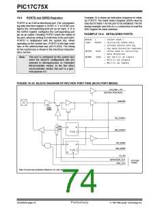
PIC17C75X
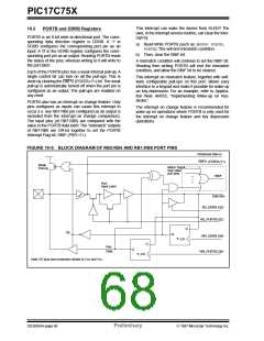
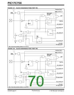
FIGURE 10-7: BLOCK DIAGRAM OF RB6 PORT PIN
Peripheral Data in
(PORTA<7>)
RBPU
Weak
Pull-Up
Match Signal
from other
port pins
RBIF
D
Q
Data Bus
EN
RD_DDRB (Q2)
RD_PORTB (Q2)
D
OE
Q
WR_DDRB (Q4)
CK
P
N
0
1
Port
Data
Q
D
WR_PORTB (Q4)
CK
Q
SPI output
SPI output enable
Note: I/O pins have protection diodes to VDD and Vss.
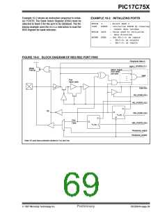
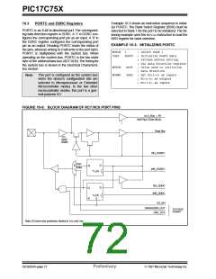
FIGURE 10-8: BLOCK DIAGRAM OF RB7 PORT PIN
Peripheral Data in
(PORTA<7>)
RBPU
Weak
Pull-Up
Match Signal
from other
port pins
RBIF
D
Q
Data Bus
EN
EN
RD_DDRB (Q2)
RD_PORTB (Q2)
D
Q
OE
WR_DDRB (Q4)
SS output disable
CK
P
N
0
1
Port
Data
Q
D
WR_PORTB (Q4)
CK
Q
SPI output
SPI output enable
Note: I/O pins have protection diodes to VDD and Vss.
DS30264A-page 70
Preliminary
1997 Microchip Technology Inc.

 MICROCHIP [ MICROCHIP ]