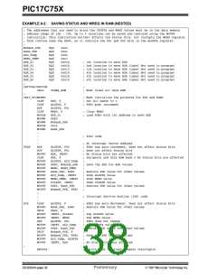
PIC17C75X
7.2.1
GENERAL PURPOSE REGISTER (GPR)
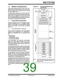
7.2
Data Memory Organization
All devices have some amount of GPR area.The GPRs
are 8-bits wide. When the GPR area is greater than
232, it must be banked to allow access to the additional
memory space.
Data memory is partitioned into two areas. The first is
the General Purpose Registers (GPR) area, while the
second is the Special Function Registers (SFR) area.
The SFRs control and give the status for the operation
of the device.
All the PIC17C75X devices have banked memory in
the GPR area. To facilitate switching between these
banks, the MOVLR bankinstruction has been added to
the instruction set. GPRs are not initialized by a
Power-on Reset and are unchanged on all other resets.
Portions of data memory are banked, this occurs in
both areas. The GPR area is banked to allow greater
than 232 bytes of general purpose RAM.
Banking requires the use of control bits for bank selec-
tion. These control bits are located in the Bank Select
Register (BSR). If an access is made to the unbanked
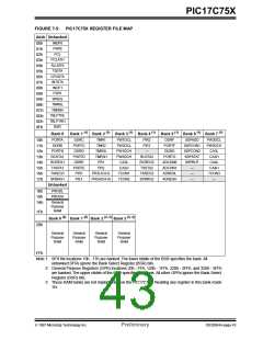
region, the BSR bits are ignored. Figure 7-5 shows the
data memory map organization.
7.2.2
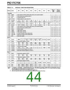
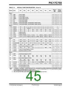
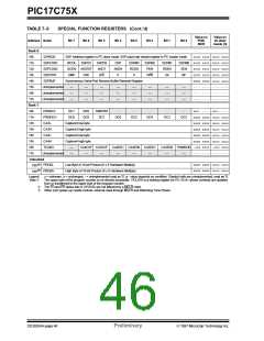
SPECIAL FUNCTION REGISTERS (SFR)
The SFRs are used by the CPU and peripheral func-
tions to control the operation of the device (Figure 7-5).
These registers are static RAM.
Instructions MOVPF and MOVFP provide the means to
move values from the peripheral area (“P”) to any loca-
tion in the register file (“F”), and vice-versa. The defini-
tion of the “P” range is from 0h to 1Fh, while the “F”
range is 0h to FFh. The “P” range has six more loca-
tions than peripheral registers which can be used as
General Purpose Registers.This can be useful in some
applications where variables need to be copied to other
locations in the general purpose RAM (such as saving
status information during an interrupt).
The SFRs can be classified into two sets, those asso-
ciated with the “core” function and those related to the
peripheral functions. Those registers related to the
“core” are described here, while those related to a
peripheral feature are described in the section for each
peripheral feature.
The peripheral registers are in the banked portion of
memory, while the core registers are in the unbanked
region. To facilitate switching between the peripheral
banks, the MOVLB bankinstruction has been provided.
The entire data memory can be accessed either
directly or indirectly through file select registers FSR0
and FSR1 (Section 7.4). Indirect addressing uses the
appropriate control bits of the BSR for accesses into
the banked areas of data memory. The BSR is
explained in greater detail in Section 7.8.
DS30264A-page 42
Preliminary
1997 Microchip Technology Inc.

 MICROCHIP [ MICROCHIP ]