PIC17C75X
7.1.2
EXTERNAL MEMORY INTERFACE
In extended microcontroller mode, when the device is
executing out of internal memory, the control signals
will continue to be active. That is, they indicate the
action that is occurring in the internal memory. The
external memory access is ignored.
When either microprocessor or extended microcontrol-
ler mode is selected, PORTC, PORTD and PORTE are
configured as the system bus. PORTC and PORTD are
the multiplexed address/data bus and PORTE<2:0> is
for the control signals. External components are
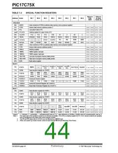
needed to demultiplex the address and data. This can
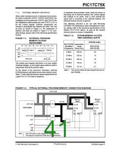
be done as shown in Figure 7-4. The waveforms of
address and data are shown in Figure 7-3. For com-
plete timings, please refer to the electrical specification
section.
This following selection is for use with Microchip
EPROMs. For interfacing to other manufacturers mem-
ory, please refer to the electrical specifications of the
desired PIC17C75X device, as well as the desired
memory device to ensure compatibility.
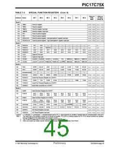
TABLE 7-2:
EPROM MEMORY ACCESS
TIME ORDERING SUFFIX
FIGURE 7-3: EXTERNAL PROGRAM
MEMORY ACCESS
EPROM Suffix
WAVEFORMS
PIC17C75X Instruction
Oscillator Cycle
Frequency Time (TCY)
Q1 Q2
Q4 Q1 Q2
Q4 Q1
Data out
Q3
Q3
PIC17C752
PIC17C756
AD
<15:0>
Address out Data in
Address out
8 MHz
16 MHz
20 MHz
25 MHz
33 MHz
500 ns
250 ns
200 ns
160 ns
121 ns
-25
-15
-10
-70
(1)
ALE
OE
'1'
WR
Read cycle
Write cycle
The system bus requires that there is no bus conflict
(minimal leakage), so the output value (address) will be
capacitively held at the desired value.
Note 1: The access times for this requires the use of
fast SRAMs.
As the speed of the processor increases, external
EPROM memory with faster access time must be used.
Table 7-2 lists external memory speed requirements for
a given PIC17C75X device frequency.
FIGURE 7-4: TYPICAL EXTERNAL PROGRAM MEMORY CONNECTION DIAGRAM
AD15-AD0
Memory
(LSB)
Memory
(MSB)
A15-A0
AD7-AD0
373
373
Ax-A0
D7-D0
Ax-A0
PIC17CXXX
D7-D0
CE
CE
(2)
(2)
OE WR
OE WR
AD15-AD8
ALE
(1)
138
(1)
I/O
OE
WR
Note 1: Use of I/O pins is only required for paged memory.
2: This signal is unused for ROM and EPROM devices.
1997 Microchip Technology Inc.
Preliminary
DS30264A-page 41

 MICROCHIP [ MICROCHIP ]