PIC17C4X
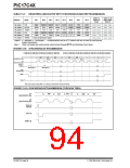
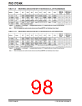
TABLE 13-9: REGISTERS ASSOCIATED WITH SYNCHRONOUS SLAVE TRANSMISSION
Value on
Power-on
Reset
Value on all
other resets
(Note1)
Address
Name
Bit 7
Bit 6
Bit 5
Bit 4
Bit 3
Bit 2
Bit 1
Bit 0
16h, Bank 1
13h, Bank 0
16h, Bank 0
17h, Bank 1
15h, Bank 0
17h, Bank 0
PIR
RBIF
SPEN
TX7
TMR3IF TMR2IF TMR1IF CA2IF
CA1IF
FERR
TX2
TXIF
OERR
TX1
RCIF
RX9D
TX0
0000 0010
0000 -00x
xxxx xxxx
0000 0000
0000 --1x
xxxx xxxx
0000 0010
0000 -00u
uuuu uuuu
0000 0000
0000 --1u
uuuu uuuu
RCSTA
TXREG
PIE
RX9
TX6
SREN
TX5
CREN
TX4
—
TX3
RBIE
CSRC
TMR3IE TMR2IE TMR1IE CA2IE
TX9 TXEN SYNC
CA1IE
—
TXIE
RCIE
TX9D
TXSTA
SPBRG
—
TRMT
Baud rate generator register
Legend: x= unknown, u= unchanged, -= unimplemented read as a '0', shaded cells are not used for synchronous
slave transmission.
Note 1: Other (non power-up) resets include: external reset through MCLR and Watchdog Timer Reset.
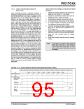
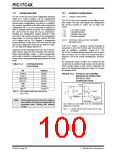
TABLE 13-10: REGISTERS ASSOCIATED WITH SYNCHRONOUS SLAVE RECEPTION
Value on
Power-on
Reset
Value on all
other resets
(Note1)
Address
Name
Bit 7
Bit 6
Bit 5
Bit 4
Bit 3
Bit 2
Bit 1
Bit 0
16h, Bank1
13h, Bank0
14h, Bank0
17h, Bank1
15h, Bank 0
17h, Bank0
PIR
RBIF
SPEN
RX7
TMR3IF TMR2IF TMR1IF CA2IF
CA1IF
FERR
RX2
TXIF
OERR
RX1
RCIF
RX9D
RX0
0000 0010
0000 -00x
xxxx xxxx
0000 0000
0000 --1x
xxxx xxxx
0000 0010
0000 -00u
uuuu uuuu
0000 0000
0000 --1u
uuuu uuuu
RCSTA
RCREG
PIE
RX9
RX6
SREN
RX5
CREN
RX4
—
RX3
RBIE
CSRC
TMR3IE TMR2IE TMR1IE CA2IE
TX9 TXEN SYNC
CA1IE
—
TXIE
RCIE
TX9D
TXSTA
SPBRG
—
TRMT
Baud rate generator register
Legend: x= unknown, u= unchanged, -= unimplemented read as a '0', shaded cells are not used for synchronous
slave reception.
Note 1: Other (non power-up) resets include: external reset through MCLR and Watchdog Timer Reset.
DS30412C-page 98
1996 Microchip Technology Inc.

 MICROCHIP [ MICROCHIP ]