PIC17C4X
9.5
I/O Programming Considerations
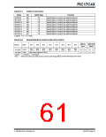
EXAMPLE 9-5: READ MODIFY WRITE
INSTRUCTIONS ON AN
I/O PORT
9.5.1
BI-DIRECTIONAL I/O PORTS
Any instruction which writes, operates internally as a
read followed by a write operation. For example, the
BCF and BSF instructions read the register into the
CPU, execute the bit operation, and write the result
back to the register. Caution must be used when these
instructions are applied to a port with both inputs and
outputs defined. For example, a BSFoperation on bit5
of PORTB will cause all eight bits of PORTB to be read
into the CPU. Then the BSF operation takes place on
bit5 and PORTB is written to the output latches. If
another bit of PORTB is used as a bi-directional I/O pin
(e.g. bit0) and it is defined as an input at this time, the
input signal present on the pin itself would be read into
the CPU and re-written to the data latch of this particu-
lar pin, overwriting the previous content. As long as the
pin stays in the input mode, no problem occurs. How-
ever, if bit0 is switched into output mode later on, the
content of the data latch may now be unknown.
; Initial PORT settings: PORTB<7:4> Inputs
;
PORTB<3:0> Outputs
; PORTB<7:6> have pull-ups and are
; not connected to other circuitry
;
;
;
;
PORT latch PORT pins
---------- ---------
BCF
BCF
PORTB, 7
PORTB, 6
01pp pppp
10pp pppp
11pp pppp
11pp pppp
;
;
BCF
BCF
DDRB, 7
DDRB, 6
10pp pppp
10pp pppp
11pp pppp
10pp pppp
; Note that the user may have expected the
; pin values to be 00pp pppp. The 2nd BCF
; caused RB7 to be latched as the pin value
; (High).
Note: A pin actively outputting a Low or High
should not be driven from external devices
in order to change the level on this pin (i.e.
“wired-or”, “wired-and”). The resulting high
output currents may damage the device.
Reading a port reads the values of the port pins.Writing
to the port register writes the value to the port latch.
When using read-modify-write instructions (BCF, BSF,
BTG, etc.) on a port, the value of the port pins is read,
the desired operation is performed with this value, and
the value is then written to the port latch.
9.5.2
SUCCESSIVE OPERATIONS ON I/O PORTS
Example 9-5 shows the effect of two sequential
read-modify-write instructions on an I/O port.
The actual write to an I/O port happens at the end of an
instruction cycle, whereas for reading, the data must be
valid at the beginning of the instruction cycle (Figure 9-
9).Therefore, care must be exercised if a write followed
by a read operation is carried out on the same I/O port.
The sequence of instructions should be such to allow
the pin voltage to stabilize (load dependent) before
executing the instruction that reads the values on that
I/O port. Otherwise, the previous state of that pin may
be read into the CPU rather than the “new” state. When
in doubt, it is better to separate these instructions with
a NOPor another instruction not accessing this I/O port.
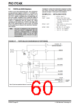
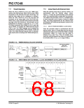
FIGURE 9-9: SUCCESSIVE I/O OPERATION
Q4
Q4
Q4
Q1 Q2
Q4
Q3
Q3
Q3
Q3
Q1 Q2
Q1 Q2
Q1 Q2
Note:
PC + 3
NOP
This example shows a write to PORTB
followed by a read from PORTB.
Note that:
data setup time = (0.25 TCY - TPD)
where TCY = instruction cycle.
TPD = propagation delay
Therefore, at higher clock
frequencies, a write followed by a
read may be problematic.
PC
PC + 1
PC + 2
NOP
Instruction
fetched
MOVWF PORTB MOVF PORTB,W
write to
PORTB
RB7:RB0
Port pin
sampled here
Instruction
executed
MOVWF PORTB MOVF PORTB,W
NOP
write to
PORTB
DS30412C-page 64
1996 Microchip Technology Inc.

 MICROCHIP [ MICROCHIP ]