PIC17C4X
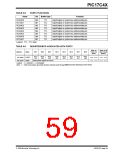
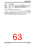
TABLE 9-9:
Name
PORTE FUNCTIONS
Bit
Buffer Type
Function
RE0/ALE
RE1/OE
RE2/WR
bit0
bit1
bit2
TTL
TTL
TTL
Input/Output or system bus Address Latch Enable (ALE) control pin.
Input/Output or system bus Output Enable (OE) control pin.
Input/Output or system bus Write (WR) control pin.
Legend: TTL = TTL input.
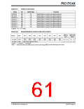
TABLE 9-10: REGISTERS/BITS ASSOCIATED WITH PORTE
Value on
Power-on
Reset
Value on all
other resets
(Note1)
Address
Name
Bit 7
Bit 6
Bit 5
Bit 4
Bit 3
Bit 2
Bit 1
Bit 0
15h, Bank 1 PORTE
14h, Bank 1 DDRE
—
—
—
—
—
RE2/WR RE1/OE RE0/ALE ---- -xxx
---- -uuu
---- -111
Data direction register for PORTE
---- -111
Legend: x= unknown, u= unchanged, - = unimplemented read as '0'. Shaded cells are not used by PORTE.
Note 1: Other (non power-up) resets include: external reset through MCLR and the Watchdog Timer Reset.
1996 Microchip Technology Inc.
DS30412C-page 63

 MICROCHIP [ MICROCHIP ]