PIC17C4X
11.1
Timer0 Operation
11.2
Using Timer0 with External Clock
When the T0CS (T0STA<5>) bit is set, TMR0 incre-
ments on the internal clock.When T0CS is clear, TMR0
increments on the external clock (RA1/T0CKI pin). The
external clock edge can be configured in software.
When the T0SE (T0STA<6>) bit is set, the timer will
increment on the rising edge of the RA1/T0CKI pin.
When T0SE is clear, the timer will increment on the fall-
ing edge of the RA1/T0CKI pin. The prescaler can be
programmed to introduce a prescale of 1:1 to 1:256.
The timer increments from 0000h to FFFFh and rolls
over to 0000h. On overflow, the TMR0 Interrupt Flag bit
(T0IF) is set. The TMR0 interrupt can be masked by
clearing the corresponding TMR0 Interrupt Enable bit
(T0IE). The TMR0 Interrupt Flag bit (T0IF) is automati-
cally cleared when vectoring to the TMR0 interrupt vec-
tor.
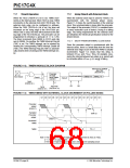
When the external clock input is used for Timer0, it is
synchronized with the internal phase clocks.
Figure 11-3 shows the synchronization of the external
clock. This synchronization is done after the prescaler.
The output of the prescaler (PSOUT) is sampled twice
in every instruction cycle to detect a rising or a falling
edge. The timing requirements for the external clock
are detailed in the electrical specification section for the
desired device.
11.2.1 DELAY FROM EXTERNAL CLOCK EDGE
Since the prescaler output is synchronized with the
internal clocks, there is a small delay from the time the
external clock edge occurs to the time TMR0 is actually
incremented. Figure 11-3 shows that this delay is
between 3TOSC and 7TOSC. Thus, for example, mea-
suring the interval between two edges (e.g. period) will
be accurate within ±4TOSC (±121 ns @ 33 MHz).
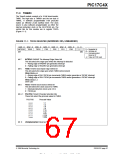
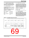
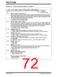
FIGURE 11-2: TIMER0 MODULE BLOCK DIAGRAM
Interrupt on overflow
sets T0IF
(INTSTA<5>)
Prescaler
0
(8 stage
Synchronization
TMR0H<8> TMR0L<8>
RA1/T0CKI
async ripple
counter)
Fosc/4
1
PSOUT
T0SE
(T0STA<6>)
4
Q2
Q4
PS3:PS0
(T0STA<4:1>)
T0CS
(T0STA<5>)
FIGURE 11-3: TMR0 TIMING WITH EXTERNAL CLOCK (INCREMENT ON FALLING EDGE)
Q1 Q2 Q3 Q4 Q1 Q2 Q3 Q4 Q1 Q2 Q3 Q4 Q1 Q2 Q3 Q4
Prescaler
output
(PSOUT)
(note 3)
(note 2)
Sampled
Prescaler
output
(note 1)
Increment
TMR0
T0
T0 + 1
T0 + 2
TMR0
Note 1: The delay from the T0CKI edge to the TMR0 increment is 3Tosc to 7Tosc.
2: ↑ = PSOUT is sampled here.
3: The PSOUT high time is too short and is missed by the sampling circuit.
DS30412C-page 68
1996 Microchip Technology Inc.

 MICROCHIP [ MICROCHIP ]