PIC17C4X
5.5
RA0/INT Interrupt
5.7
T0CKI Interrupt
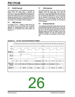
The external interrupt on the RA0/INT pin is edge trig-
gered. Either the rising edge, if INTEDG bit
(T0STA<7>) is set, or the falling edge, if INTEDG bit is
clear. When a valid edge appears on the RA0/INT pin,
the INTF bit (INTSTA<4>) is set. This interrupt can be
disabled by clearing the INTE control bit (INTSTA<0>).
The INT interrupt can wake the processor from SLEEP.
See Section 14.4 for details on SLEEP operation.
The external interrupt on the RA1/T0CKI pin is edge
triggered. Either the rising edge, if the T0SE bit
(T0STA<6>) is set, or the falling edge, if the T0SE bit is
clear. When a valid edge appears on the RA1/T0CKI
pin, the T0CKIF bit (INTSTA<6>) is set. This interrupt
can be disabled by clearing the T0CKIE control bit
(INTSTA<2>). The T0CKI interrupt can wake up the
processor from SLEEP. See Section 14.4 for details on
SLEEP operation.
5.6
TMR0 Interrupt
5.8
Peripheral Interrupt
An overflow (FFFFh → 0000h) in TMR0 will set the
T0IF (INTSTA<5>) bit. The interrupt can be enabled/
disabled by setting/clearing the T0IE control bit
(INTSTA<1>). For operation of the Timer0 module, see
Section 11.0.
The peripheral interrupt flag indicates that at least one
of the peripheral interrupts occurred (PEIF is set). The
PEIF bit is a read only bit, and is a bit wise OR of all the
flag bits in the PIR register AND’ed with the corre-
sponding enable bits in the PIE register. Some of the
peripheral interrupts can wake the processor from
SLEEP. See Section 14.4 for details on SLEEP opera-
tion.
FIGURE 5-5: INT PIN / T0CKI PIN INTERRUPT TIMING
Q1 Q2 Q3 Q4 Q1 Q2 Q3 Q4 Q1 Q2 Q3 Q4 Q1 Q2 Q3 Q4 Q1 Q2 Q3 Q4 Q1 Q2 Q3 Q4 Q1 Q2 Q3 Q4
OSC1
OSC2
RA0/INT or
RA1/T0CKI
INTF or
T0CKIF
GLINTD
PC
PC
PC + 1
Addr (Vector)
YY
YY + 1
PC + 1
System Bus
Instruction
Fetched
Addr
Addr
Addr
Addr
Addr
Inst (YY + 1)
PC Inst (PC)
Inst (PC+1)
Inst (Vector)
Inst (PC+1)
RETFIE
Instruction
executed
Dummy
Inst (PC)
Dummy
Dummy
RETFIE
DS30412C-page 26
1996 Microchip Technology Inc.

 MICROCHIP [ MICROCHIP ]