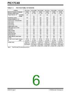
PIC17C4X
The PIC17CXX devices contain an 8-bit ALU and work-
ing register. The ALU is a general purpose arithmetic
unit. It performs arithmetic and Boolean functions
between data in the working register and any register
file.
3.0
ARCHITECTURAL OVERVIEW
The high performance of the PIC17C4X can be attrib-
uted to a number of architectural features commonly
found in RISC microprocessors. To begin with, the
PIC17C4X uses a modified Harvard architecture. This
architecture has the program and data accessed from
separate memories. So the device has a program
memory bus and a data memory bus. This improves
bandwidth over traditional von Neumann architecture,
where program and data are fetched from the same
memory (accesses over the same bus). Separating
program and data memory further allows instructions to
be sized differently than the 8-bit wide data word.
PIC17C4X opcodes are 16-bits wide, enabling single
word instructions.The full 16-bit wide program memory
bus fetches a 16-bit instruction in a single cycle. A two-
stage pipeline overlaps fetch and execution of instruc-
tions. Consequently, all instructions execute in a single
cycle (121 ns @ 33 MHz), except for program branches
and two special instructions that transfer data between
program and data memory.
The ALU is 8-bits wide and capable of addition, sub-
traction, shift, and logical operations. Unless otherwise
mentioned, arithmetic operations are two's comple-
ment in nature.
The WREG register is an 8-bit working register used for
ALU operations.
All PIC17C4X devices (except the PIC17C42) have an
8 x 8 hardware multiplier. This multiplier generates a
16-bit result in a single cycle.
Depending on the instruction executed, the ALU may
affect the values of the Carry (C), Digit Carry (DC), and
Zero (Z) bits in the STATUS register.The C and DC bits
operate as a borrow and digit borrow out bit, respec-
tively, in subtraction. See the SUBLW and SUBWF
instructions for examples.
Although the ALU does not perform signed arithmetic,
the Overflow bit (OV) can be used to implement signed
math. Signed arithmetic is comprised of a magnitude
and a sign bit. The overflow bit indicates if the magni-
tude overflows and causes the sign bit to change state.
Signed math can have greater than 7-bit values (mag-
nitude), if more than one byte is used. The use of the
overflow bit only operates on bit6 (MSb of magnitude)
and bit7 (sign bit) of the value in the ALU. That is, the
overflow bit is not useful if trying to implement signed
math where the magnitude, for example, is 11-bits. If
the signed math values are greater than 7-bits (15-, 24-
or 31-bit), the algorithm must ensure that the low order
bytes ignore the overflow status bit.
The PIC17C4X can address up to 64K x 16 of program
memory space.
The PIC17C42 and PIC17C42A integrate 2K x 16 of
EPROM program memory on-chip, while the
PIC17CR42 has 2K x 16 of ROM program memory on-
chip.
The PIC17C43 integrates 4K x 16 of EPROM program
memory, while the PIC17CR43 has 4K x 16 of ROM
program memory.
The PIC17C44 integrates 8K x 16 EPROM program
memory.
Program execution can be internal only (microcontrol-
ler or protected microcontroller mode), external only
(microprocessor mode) or both (extended microcon-
troller mode). Extended microcontroller mode does not
allow code protection.
Care should be taken when adding and subtracting
signed numbers to ensure that the correct operation is
executed. Example 3-1 shows an item that must be
taken into account when doing signed arithmetic on an
ALU which operates as an unsigned machine.
The PIC17CXX can directly or indirectly address its
register files or data memory. All special function regis-
ters, including the Program Counter (PC) and Working
Register (WREG), are mapped in the data memory.
The PIC17CXX has an orthogonal (symmetrical)
instruction set that makes it possible to carry out any
operation on any register using any addressing mode.
This symmetrical nature and lack of ‘special optimal sit-
uations’ make programming with the PIC17CXX simple
yet efficient. In addition, the learning curve is reduced
significantly.
EXAMPLE 3-1: SIGNED MATH
Hex Value
Signed Value
Math
Unsigned Value
Math
FFh
-127
255
+ 01h
+
1
+
=
1
=
?
= -126 (FEh)
0 (00h);
Carry bit = 1
Signed math requires the result in REG to
be FEh (-126). This would be accomplished
by subtracting one as opposed to adding
one.
One of the PIC17CXX family architectural enhance-
ments from the PIC16CXX family allows two file regis-
ters to be used in some two operand instructions. This
allows data to be moved directly between two registers
without going through the WREG register. This
increases performance and decreases program mem-
ory usage.
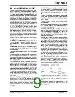
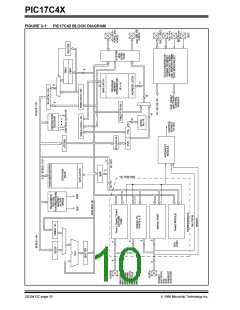
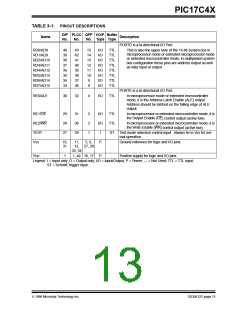
Simplified block diagrams are shown in Figure 3-1 and
Figure 3-2. The descriptions of the device pins are
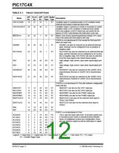
listed in Table 3-1.
1996 Microchip Technology Inc.
DS30412C-page 9
This document was created with FrameMaker 4 0 4

 MICROCHIP [ MICROCHIP ]