PIC17C4X
14.3.2 CLEARING THE WDT AND POSTSCALER
The WDT and postscaler are cleared when:
14.3
Watchdog Timer (WDT)
The Watchdog Timer’s function is to recover from soft-
ware malfunction. The WDT uses an internal free run-
ning on-chip RC oscillator for its clock source. This
does not require any external components. This RC
oscillator is separate from the RC oscillator of the
OSC1/CLKIN pin. That means that the WDT will run,
even if the clock on the OSC1/CLKIN and OSC2/CLK-
OUT pins of the device has been stopped, for example,
by execution of a SLEEP instruction. During normal
operation and SLEEP mode, a WDT time-out gener-
ates a device RESET. The WDT can be permanently
disabled by programming the configuration bits
WDTPS1:WDTPS0 as '00' (Section 14.1).
• The device is in the reset state
• A SLEEPinstruction is executed
• A CLRWDTinstruction is executed
• Wake-up from SLEEP by an interrupt
The WDT counter/postscaler will start counting on the
first edge after the device exits the reset state.
14.3.3 WDT PROGRAMMING CONSIDERATIONS
It should also be taken in account that under worst case
conditions (VDD = Min., Temperature = Max., max.
WDT postscaler) it may take several seconds before a
WDT time-out occurs.
Under normal operation, the WDT must be cleared on
a regular interval. This time is less the minimum WDT
overflow time. Not clearing the WDT in this time frame
will cause the WDT to overflow and reset the device.
The WDT and postscaler is the Power-up Timer during
the Power-on Reset sequence.
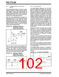
14.3.4 WDT AS NORMAL TIMER
14.3.1 WDT PERIOD
When the WDT is selected as a normal timer, the clock
source is the device clock. Neither the WDT nor the
postscaler are directly readable or writable. The over-
flow time is 65536 TOSC cycles. On overflow, the TO bit
is cleared (device is not reset). The CLRWDTinstruction
can be used to set the TO bit. This allows the WDT to
be a simple overflow timer. When in sleep, the WDT
does not increment.
The WDT has a nominal time-out period of 12 ms, (with
postscaler = 1). The time-out periods vary with temper-
DD
ature, V and process variations from part to part (see
DC specs). If longer time-out periods are desired, a
postscaler with a division ratio of up to 1:256 can be
assigned to the WDT. Thus, typical time-out periods up
to 3.0 seconds can be realized.
The CLRWDT and SLEEP instructions clear the WDT
and the postscaler (if assigned to the WDT) and pre-
vent it from timing out thus generating a device RESET
condition.
The TO bit in the CPUSTA register will be cleared upon
a WDT time-out.
1996 Microchip Technology Inc.
DS30412C-page 103

 MICROCHIP [ MICROCHIP ]