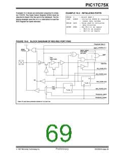
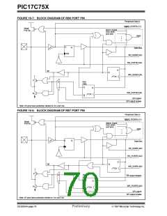
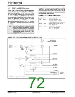
PIC17C75X
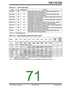
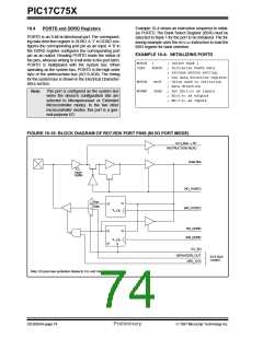
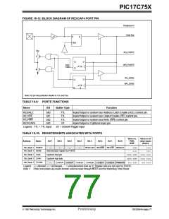
TABLE 10-5: PORTC FUNCTIONS
Name
RC0/AD0
Bit
Buffer Type
Function
bit0
bit1
bit2
bit3
bit4
bit5
bit6
bit7
TTL
TTL
TTL
TTL
TTL
TTL
TTL
TTL
Input/Output or system bus address/data pin.
Input/Output or system bus address/data pin.
Input/Output or system bus address/data pin.
Input/Output or system bus address/data pin.
Input/Output or system bus address/data pin.
Input/Output or system bus address/data pin.
Input/Output or system bus address/data pin.
Input/Output or system bus address/data pin.
RC1/AD1
RC2/AD2
RC3/AD3
RC4/AD4
RC5/AD5
RC6/AD6
RC7/AD7
Legend: TTL = TTL input.
TABLE 10-6: REGISTERS/BITS ASSOCIATED WITH PORTC
Value on
POR,
BOR
Value on all
other resets
(Note1)
Address
Name
Bit 7
Bit 6
Bit 5
Bit 4
Bit 3
Bit 2
Bit 1
Bit 0
RC7/
AD7
RC6/
AD6
RC5/
AD5
RC4/
AD4
RC3/
AD3
RC2/
AD2
RC1/
AD1
RC0/
AD0
11h, Bank 1 PORTC
10h, Bank 1 DDRC
xxxx xxxx
1111 1111
uuuu uuuu
1111 1111
Data direction register for PORTC
Legend: x= unknown, u= unchanged.
Note 1: Other (non power-up) resets include: external reset through MCLR and the Watchdog Timer Reset.
1997 Microchip Technology Inc.
Preliminary
DS30264A-page 73

 MICROCHIP [ MICROCHIP ]