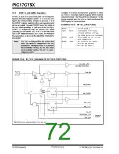
PIC17C75X
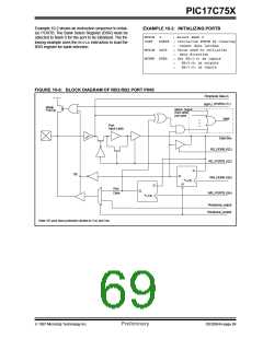
Example 10-3 shows an instruction sequence to initial-
ize PORTC. The Bank Select Register (BSR) must be
selected to Bank 1 for the port to be initialized. The fol-
lowing example uses the MOVLBinstruction to load the
BSR register for bank selection.
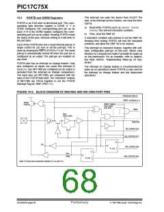
10.3
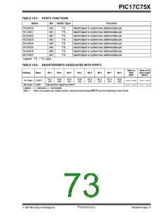
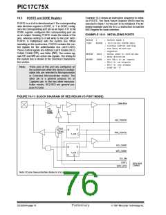
PORTC and DDRC Registers
PORTC is an 8-bit bi-directional port. The correspond-
ing data direction register is DDRC. A '1' in DDRC con-
figures the corresponding port pin as an input. A '0' in
the DDRC register configures the corresponding port
pin as an output. Reading PORTC reads the status of
the pins, whereas writing to it will write to the port latch.
PORTC is multiplexed with the system bus. When
operating as the system bus, PORTC is the low order
byte of the address/data bus (AD7:AD0).The timing for
the system bus is shown in the Electrical Characteris-
tics section.
EXAMPLE 10-3: INITIALIZING PORTC
MOVLB
CLRF
1
; Select Bank 1
PORTC ; Initialize PORTC data
; latches before setting
; the data direction register
MOVLW
MOVWF
0xCF
; Value used to initialize
; data direction
DDRC ; Set RC<3:0> as inputs
; RC<5:4> as outputs
Note: This port is configured as the system bus
when the device’s configuration bits are
selected to Microprocessor or Extended
Microcontroller modes. In the two other
microcontroller modes, this port is a gen-
eral purpose I/O.
; RC<7:6> as inputs
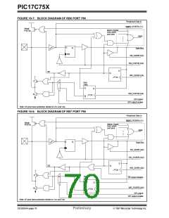
FIGURE 10-9: BLOCK DIAGRAM OF RC7:RC0 PORT PINS
to D_Bus → IR
INSTRUCTION READ
Data Bus
TTL
Input
Buffer
RD_PORTC
WR_PORTC
Port
D
D
0
1
Q
Data
CK
RD_DDRC
WR_DDRC
Q
R
CK
S
EX_EN
DATA/ADDR_OUT
SYS BUS
Control
DRV_SYS
Note: I/O pins have protection diodes to VDD and Vss.
DS30264A-page 72
Preliminary
1997 Microchip Technology Inc.

 MICROCHIP [ MICROCHIP ]