PIC17C75X
10.1
PORTA Register
10.0 I/O PORTS
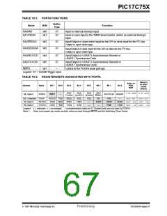
PIC17C75X devices have seven I/O ports, PORTA
through PORTG. PORTB through PORTG have a cor-
responding Data Direction Register (DDR), which is
used to configure the port pins as inputs or outputs.
These seven ports are made up of 50 I/O pins. Some
of these ports pins are multiplexed with alternate func-
tions.
PORTA is a 6-bit wide latch. PORTA does not have a
corresponding Data Direction Register (DDR).
Reading PORTA reads the status of the pins.
The RA1 pin is multiplexed with TMR0 clock input, RA2
and RA3 are multiplexed with the SSP functions, and
RA4 and RA5 are multiplexed with the USART1 func-
tions. The control of RA2, RA3, RA4 and RA5 as out-
puts are automatically configured by the their
multiplexed peripheral module.
PORTC, PORTD, and PORTE are multiplexed with the
system bus. These pins are configured as the system
bus when the device’s configuration bits are selected to
Microprocessor or Extended Microcontroller modes. In
the two other microcontroller modes, these pins are
general purpose I/O.
10.1.1 USING RA2, RA3 AS OUTPUTS
The RA2 and RA3 pins are open drain outputs. To use
the RA2 and/or the RA3 pin(s) as output(s), simply
write to the PORTA register the desired value. A '0' will
cause the pin to drive low, while a '1' will cause the pin
to float (hi-impedance). An external pull-up resistor
should be used to pull the pin high. Writes to the RA2
and RA3 pins will not affect the other PORTA pins.
PORTA, PORTB, PORTE<3>, PORTF and PORTG
are multiplexed with the peripheral features of the
device. These peripheral features are:
• Timer modules
• Capture modules
• PWM modules
• USART/SCI modules
• SSP Module
Note: When using the RA2 or RA3 pin(s) as out-
put(s), read-modify-write instructions (such
as BCF, BSF, BTG) on PORTA are not rec-
ommended.
• A/D Module
• External Interrupt pin
Such operations read the port pins, do the
desired operation, and then write this value
to the data latch. This may inadvertently
cause the RA2 or RA3 pins to switch from
input to output (or vice-versa).
To avoid this possibility use a shadow reg-
ister for PORTA. Do the bit operations on
this shadow register and then move it to
PORTA.
When some of these peripheral modules are turned on,
the port pin will automatically configure to the alternate
function. The modules that do this are:
• PWM module
• SSP module
• USART/SCI module
When a pin is automatically configured as an output by
a peripheral module, the pins data direction (DDR) bit
is unknown. After disabling the peripheral module, the
user should re-initialize the DDR bit to the desired con-
figuration.
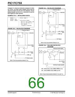
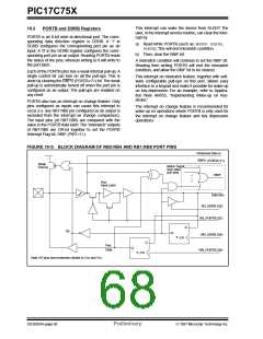
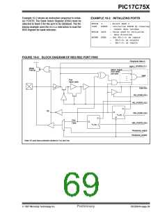
FIGURE 10-1: RA0 AND RA1 BLOCK
DIAGRAM
The other peripheral modules (which require an input)
must have their data direction bit configured appropri-
ately.
DATA BUS
Note: A pin that is a peripheral input, can be con-
figured as an output (DDRx<y> is cleared).
The peripheral events will be determined
by the action output on the port pin.
RD_PORTA
(Q2)
Note: I/O pins have protection diodes to VDD and VSS.
1997 Microchip Technology Inc.
Preliminary
DS30264A-page 65

 MICROCHIP [ MICROCHIP ]