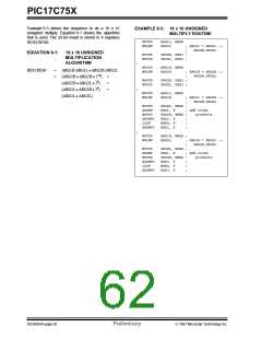
PIC17C75X
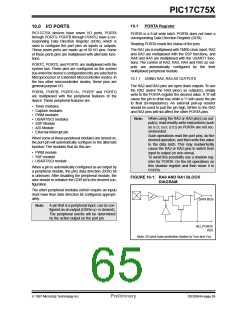
Example 10-1 shows an instruction sequence to initial-
ize PORTA. The Bank Select Register (BSR) must be
selected to Bank 0 for the port to be initialized. The fol-
lowing example uses the MOVLBinstruction to load the
BSR register for bank selection.
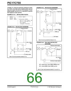
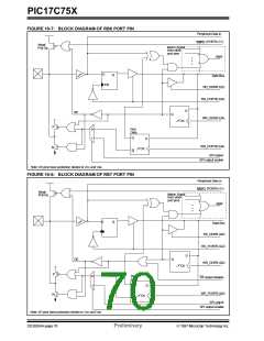
FIGURE 10-3: RA3 BLOCK DIAGRAM
Peripheral data in
D
Q
Data Bus
EN
EXAMPLE 10-1: INITIALIZING PORTA
MOVLB
MOVLW 0xF3
0
; Select Bank 0
;
MOVPF PORTA ; Initialize PORTA
;
;
;
;
RA<3:2> are output low
RA<5:4> and RA<1:0>
are inputs
RD_PORTA
(Q2)
(outputs floating)
Q
D
FIGURE 10-2: RA2 BLOCK DIAGRAM
Peripheral data in
WR_PORTA
(Q4)
Q
CK
D
Q
Data Bus
SDA out
“1”
EN
SSP Mode
Note: I/O pin has protection diodes to VSS.
RD_PORTA
(Q2)
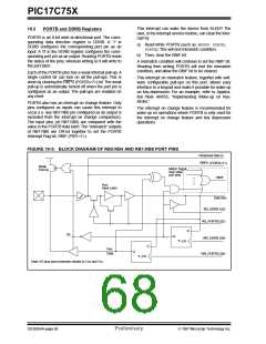
FIGURE 10-4: RA4 AND RA5 BLOCK
DIAGRAM
Q
D
Serial port input signal
WR_PORTA
(Q4)
Q
1
0
CK
Data Bus
SCL out
2
I C Mode enable
Note: I/O pin has protection diodes to VSS.
RD_PORTA
(Q2)
Serial port output signals
OE = SPEN,SYNC,TXEN, CREN, SREN for RA4
OE = SPEN (SYNC+SYNC,CSRC) for RA5
Note: I/O pins have protection diodes to VDD and VSS.
DS30264A-page 66
Preliminary
1997 Microchip Technology Inc.

 MICROCHIP [ MICROCHIP ]