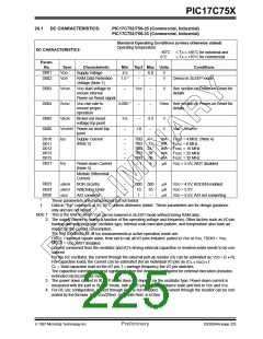
PIC17C75X
20.2
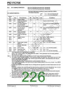
DC CHARACTERISTICS:
PIC17LC752/756 (Commercial, Industrial)
PIC17LC752/756 (Commercial, Industrial)
Standard Operating Conditions (unless otherwise stated)
Operating temperature
DC CHARACTERISTICS
Param.
-40˚C
0˚C
≤ TA ≤ +85˚C for industrial and
≤ TA ≤ +70˚C for commercial
No.
Sym
Characteristic
Min
Typ† Max Units
Conditions
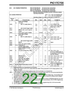
D001
D002
VDD
Supply Voltage
3.0
–
–
6.0
–
V
V
VDR
RAM Data Retention
Voltage (Note 1)
1.5 *
Device in SLEEP mode
D003
D004
VPOR
VDD start voltage to
ensure internal
Power-on Reset signal
–
VSS
–
–
–
V
See section on Power-on Reset for
details
SVDD
VBOR
VDD rise rate to
ensure proper
operation
0.010 *
V/ms See section on Power-on Reset for
details
D005
D006
Brown-out Reset
voltage trip point
3.6
–
–
4.3
–
V
VPORTP Power-on reset trip
point
1.8
V
VDD = VPORTP
D010
D011
D014
IDD
Supply Current
(Note 2)
–
–
–
3
6
85
6 *
12
150
mA FOSC = 4 MHz (Note 4)
mA
FOSC = 8 MHz
µA
FOSC = 32 kHz,
(EC osc configuration)
D021
IPD
Power-down Current
(Note 3)
–
< 1
5
µA
VDD = 5.5V, WDT disabled
Module Differential
Current
D023
D024
D026
∆IBOR
∆IWDT
∆IAD
BOR circuitry
Watchdog Timer
A/D converter
–
–
–
300 500
µA
µA
µA
VDD = 4.5V, BODEN enabled
VDD = 5.5V
10
1
35
–
VDD = 5.5V, A/D not converting
*
These parameters are characterized but not tested.
†
Data in "Typ" column is at 5V, 25˚C unless otherwise stated. These parameters are for design guidance
only and are not tested.
Note 1: This is the limit to which VDD can be lowered in SLEEP mode without losing RAM data.
2: The supply current is mainly a function of the operating voltage and frequency. Other factors such as I/O pin
loading and switching rate, oscillator type, internal code execution pattern, and temperature also have an
impact on the current consumption.
The test conditions for all IDD measurements in active operation mode are:
OSC1=external square wave, from rail to rail; all I/O pins tristated, pulled to VDD or VSS, T0CKI = VDD, MCLR
= VDD; WDT disabled.
Current consumed from the oscillator and I/O’s driving external capacitive or resistive loads needs to be con-
sidered.
For the RC oscillator, the current through the external pull-up resistor (R) can be estimated as: VDD / (2 • R).
For capacitive loads, the current can be estimated (for an individual I/O pin) as (CL • VDD) • f
CL = Total capacitive load on the I/O pin; f = average frequency the I/O pin switches.
The capacitive currents are most significant when the device is configured for external execution (includes
extended microcontroller mode).
3: The power down current in SLEEP mode does not depend on the oscillator type. Power-down current is
measured with the part in SLEEP mode, with all I/O pins in hi-impedance state and tied to VDD or VSS.
4: For RC osc configuration, current through Rext is not included. The current through the resistor can be esti-
mated by the formula IR = VDD/2Rext (mA) with Rext in kOhm.
DS30264A-page 226
Preliminary
1997 Microchip Technology Inc.

 MICROCHIP [ MICROCHIP ]