PIC17C75X
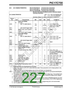
20.0 PIC17C752/756 ELECTRICAL CHARACTERISTICS
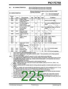
Absolute Maximum Ratings †
Ambient temperature under bias.................................................................................................................-55 to +125˚C
Storage temperature .............................................................................................................................. -65˚C to +150˚C
Voltage on VDD with respect to VSS ................................................................................................................ 0 to +7.5V
Voltage on MCLR with respect to VSS (Note 2)..........................................................................................-0.3V to +14V
Voltage on RA2 and RA3 with respect to VSS.............................................................................................-0.3V to +14V
Voltage on all other pins with respect to VSS .................................................................................... -0.3V to VDD + 0.3V
Total power dissipation (Note 1)................................................................................................................................1.0W
Maximum current out of VSS pin(s) - total (@ 70˚C) ............................................................................................500 mA
Maximum current into VDD pin(s) - total (@ 70˚C) ...............................................................................................500 mA
Input clamp current, IIK (VI < 0 or VI > VDD) ......................................................................................................................±20 mA
Output clamp current, IOK (VO < 0 or VO > VDD) ..............................................................................................................±20 mA
Maximum output current sunk by any I/O pin (except RA2 and RA3).....................................................................35 mA
Maximum output current sunk by RA2 or RA3 pins ................................................................................................60 mA
Maximum output current sourced by any I/O pin ....................................................................................................20 mA
Maximum current sunk by PORTA and PORTB (combined).................................................................................150 mA
Maximum current sourced by PORTA and PORTB (combined)............................................................................100 mA
Maximum current sunk by PORTC, PORTD and PORTE (combined)..................................................................150 mA
Maximum current sourced by PORTC, PORTD and PORTE (combined).............................................................100 mA
Maximum current sunk by PORTF and PORTG (combined) ................................................................................150 mA
Maximum current sourced by PORTF and PORTG (combined)...........................................................................100 mA
Note 1: Power dissipation is calculated as follows: Pdis = VDD x {IDD - ∑ IOH} + ∑ {(VDD-VOH) x IOH} + ∑(VOL x IOL)
Note 2: Voltage spikes below VSS at the MCLR pin, inducing currents greater than 80 mA, may cause latch-up. Thus,
a series resistor of 50-100Ω should be used when applying a "low" level to the MCLR pin rather than pulling
this pin directly to VSS.
† NOTICE: Stresses above those listed under "Absolute Maximum Ratings" may cause permanent damage to the
device. This is a stress rating only and functional operation of the device at those or any other conditions above
those indicated in the operation listings of this specification is not implied. Exposure to maximum rating conditions for
extended periods may affect device reliability.
1997 Microchip Technology Inc.
Preliminary
DS30264A-page 223

 MICROCHIP [ MICROCHIP ]