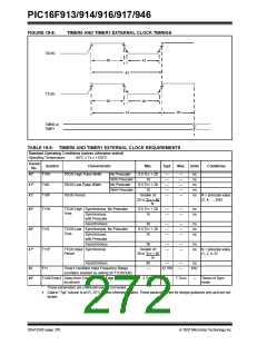
PIC16F913/914/916/917/946
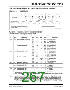
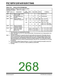
TABLE 19-2: OSCILLATOR PARAMETERS
Standard Operating Conditions (unless otherwise stated)
Operating Temperature
-40°C ≤ TA ≤ +125°C
Param
Sym.
No.
Freq.
Tolerance
Characteristic
Min.
Typ†
Max. Units
Conditions
TOSC Slowest clock
ms LFINTOSC/64
OS06
OS07
OS08
TWARM
Internal Oscillator Switch
—
—
—
2
(3)
when running
TSC
Fail-Safe Sample Clock
—
21
—
—
(1)
Period
HFOSC
Internal Calibrated
HFINTOSC Frequency
1%
2%
7.92
7.84
8.0
8.0
8.08
8.16
MHz VDD = 3.5V, 25°C
(2)
MHz 2.5V ≤ VDD ≤ 5.5V,
0°C ≤ TA ≤ +85°C
5%
—
7.60
15
8.0
31
8.40
45
MHz 2.0V ≤ VDD ≤ 5.5V,
-40°C ≤ TA ≤ +85°C (Ind.),
-40°C ≤ TA ≤ +125°C (Ext.)
OS09*
OS10*
LFOSC
Internal Uncalibrated
LFINTOSC Frequency
kHz
TIOSC
ST
HFINTOSC Oscillator
Wake-up from Sleep
Start-up Time
—
—
—
5.5
3.5
3
12
7
24
14
11
μs
μs
μs
VDD = 2.0V, -40°C to +85°C
VDD = 3.0V, -40°C to +85°C
VDD = 5.0V, -40°C to +85°C
6
*
These parameters are characterized but not tested.
†
Data in “Typ” column is at 5.0V, 25°C unless otherwise stated. These parameters are for design guidance only
and are not tested.
Note 1: Instruction cycle period (TCY) equals four times the input oscillator time base period. All specified values are
based on characterization data for that particular oscillator type under standard operating conditions with the
device executing code. Exceeding these specified limits may result in an unstable oscillator operation and/or
higher than expected current consumption. All devices are tested to operate at “min” values with an external
clock applied to the OSC1 pin. When an external clock input is used, the “max” cycle time limit is “DC” (no clock)
for all devices.
2: To ensure these oscillator frequency tolerances, VDD and VSS must be capacitively decoupled as close to the
device as possible. 0.1 μF and 0.01 μF values in parallel are recommended.
3: By design.
DS41250F-page 266
© 2007 Microchip Technology Inc.

 MICROCHIP [ MICROCHIP ]