PIC16F913/914/916/917/946
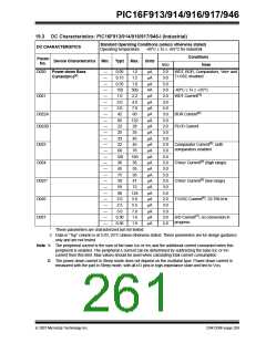
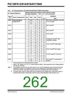
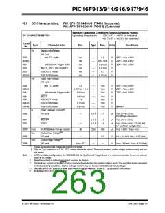
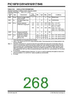
19.5 DC Characteristics: PIC16F913/914/916/917/946-I (Industrial)
PIC16F913/914/916/917/946-E (Extended) (Continued)
Standard Operating Conditions (unless otherwise stated)
DC CHARACTERISTICS
Operating temperature
-40°C ≤ TA ≤ +85°C for industrial
-40°C ≤ TA ≤ +125°C for extended
Param
No.
Sym.
Characteristic
Min.
Typ†
Max. Units
Conditions
Capacitive Loading Specs on
Output Pins
D101* COSC2 OSC2 pin
—
—
—
—
15
50
pF In XT, HS and LP modes when
external clock is used to drive
OSC1
D101A* CIO
All I/O pins
pF
Data EEPROM Memory
Byte Endurance
Byte Endurance
VDD for Read/Write
D120
ED
100K
10K
1M
100K
—
—
—
E/W -40°C ≤ TA ≤ +85°C
E/W +85°C ≤ TA ≤ +125°C
D120A ED
D121
VDRW
VMIN
5.5
V
Using EECON1 to read/write
VMIN = Minimum operating
voltage
D122
D123
TDEW
Erase/Write Cycle Time
Characteristic Retention
—
5
6
ms
TRETD
40
—
—
Year Provided no other specifications
are violated
D124
TREF
Number of Total Erase/Write
Cycles before Refresh
1M
10M
—
E/W -40°C ≤ TA ≤ +85°C
(4)
Program Flash Memory
Cell Endurance
D130
EP
10K
1K
100K
10K
—
—
—
E/W -40°C ≤ TA ≤ +85°C
E/W +85°C ≤ TA ≤ +125°C
D130A ED
Cell Endurance
D131
VPR
VDD for Read
VMIN
5.5
V
VMIN = Minimum operating
voltage
D132
D133
D134
VPEW
TPEW
TRETD
VDD for Erase/Write
4.5
—
—
—
—
5.5
3
V
Erase/Write cycle time
Characteristic Retention
ms
40
—
Year Provided no other specifications
are violated
*
These parameters are characterized but not tested.
†
Data in “Typ” column is at 5.0V, 25°C unless otherwise stated. These parameters are for design guidance only and are
not tested.
Note 1: In RC oscillator configuration, the OSC1/CLKIN pin is a Schmitt Trigger input. It is not recommended to use an external
clock in RC mode.
2: Negative current is defined as current sourced by the pin.
3: The leakage current on the MCLR pin is strongly dependent on the applied voltage level. The specified levels represent
normal operating conditions. Higher leakage current may be measured at different input voltages.
4: See Section 13.0 “Data EEPROM and Flash Program Memory Control” for additional information.
5: Including OSC2 in CLKOUT mode.
DS41250F-page 262
© 2007 Microchip Technology Inc.

 MICROCHIP [ MICROCHIP ]