PIC16F913/914/916/917/946
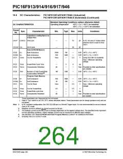
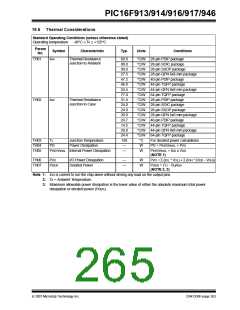
19.6 Thermal Considerations
Standard Operating Conditions (unless otherwise stated)
Operating temperature
-40°C ≤ TA ≤ +125°C
Param
Symbol
No.
Characteristic
Typ.
Units
Conditions
TH01
θJA
Thermal Resistance
Junction to Ambient
60.0
80.0
90.0
27.5
47.2
46.0
24.4
77.0
31.4
24.0
24.0
20.0
24.7
14.5
20.0
24.4
150
—
°C/W 28-pin PDIP package
°C/W 28-pin SOIC package
°C/W 28-pin SSOP package
°C/W 28-pin QFN 6x6 mm package
°C/W 40-pin PDIP package
°C/W 44-pin TQFP package
°C/W 44-pin QFN 8x8 mm package
°C/W 64-pin TQFP package
°C/W 28-pin PDIP package
°C/W 28-pin SOIC package
°C/W 28-pin SSOP package
°C/W 28-pin QFN 6x6 mm package
°C/W 40-pin PDIP package
°C/W 44-pin TQFP package
°C/W 44-pin QFN 8x8 mm package
°C/W 64-pin TQFP package
TH02
θJC
Thermal Resistance
Junction to Case
TH03
TH04
TH05
TJ
Junction Temperature
Power Dissipation
°C
W
W
For derated power calculations
PD = PINTERNAL + PI/O
PD
PINTERNAL Internal Power Dissipation
—
PINTERNAL = IDD x VDD
(NOTE 1)
TH06
TH07
PI/O
I/O Power Dissipation
Derated Power
—
—
W
W
PI/O = Σ (IOL * VOL) + Σ (IOH * (VDD - VOH))
PDER = (TJ - TA)/θJA
(NOTE 2, 3)
PDER
Note 1: IDD is current to run the chip alone without driving any load on the output pins.
2: TA = Ambient Temperature.
3: Maximum allowable power dissipation is the lower value of either the absolute maximum total power
dissipation or derated power (PDER).
© 2007 Microchip Technology Inc.
DS41250F-page 263

 MICROCHIP [ MICROCHIP ]