PIC16F913/914/916/917/946
An SSP interrupt is generated for each data transfer
14.12.3 TRANSMISSION
byte. Flag bit SSPIF must be cleared in software, and
the SSPSTAT register is used to determine the status
of the byte. Flag bit SSPIF is set on the falling edge of
the ninth clock pulse.
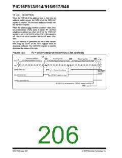
When the R/W bit of the incoming address byte is set
and an address match occurs, the R/W bit of the
SSPSTAT register is set. The received address is
loaded into the SSPBUF register. The ACK pulse will
As a slave-transmitter, the ACK pulse from the master
receiver is latched on the rising edge of the ninth SCL
input pulse. If the SDA line was high (not ACK), then
the data transfer is complete. When the ACK is latched
by the slave, the slave logic is reset (resets SSPSTAT
register) and the slave then monitors for another
occurrence of the Start bit. If the SDA line was low
(ACK), the transmit data must be loaded into the
SSPBUF register, which also loads the SSPSR
register. Then pin RC6/TX/CK/SCK/SCL/SEG9 should
be enabled by setting bit CKP.
be
sent
on
the
ninth
bit,
and
pin
RC6/TX/CK/SCK/SCL/SEG9 is held low. The transmit
data must be loaded into the SSPBUF register, which
also loads the SSPSR register. Then, pin
RC6/TX/CK/SCK/SCL/SEG9 should be enabled by
setting bit CKP of the SSPCON register. The master
must monitor the SCL pin prior to asserting another
clock pulse. The slave devices may be holding off the
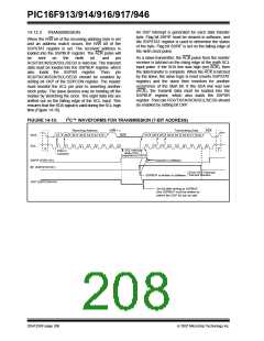
master by stretching the clock. The eight data bits are
shifted out on the falling edge of the SCL input. This
ensures that the SDA signal is valid during the SCL high
time (Figure 14-10).
FIGURE 14-10:
I2C™ WAVEFORMS FOR TRANSMISSION (7-BIT ADDRESS)
Receiving Address
R/W = 1
ACK
Transmitting Data
ACK
9
SDA
A7 A6 A5 A4 A3 A2 A1
D7 D6 D5 D4 D3 D2 D1 D0
SCL
1
2
3
4
5
6
7
8
9
1
2
3
4
5
6
7
8
S
P
SCL held low
while CPU
responds to SSPIF
Data in
sampled
Cleared in software
SSPIF (PIR1<3>)
BF (SSPSTAT<0>)
From SSP Interrupt
Service Routine
SSPBUF is written in software
CKP (SSPCON<4>)
Set bit after writing to SSPBUF
(the SSPBUF must be written to
before the CKP bit can be set)
DS41250F-page 206
© 2007 Microchip Technology Inc.

 MICROCHIP [ MICROCHIP ]