PIC16F913/914/916/917/946
an A/D acquisition must be done before the conversion
can be started. To calculate the minimum acquisition
time, Equation 12-1 may be used. This equation
assumes that 1/2 LSb error is used (1024 steps for the
ADC). The 1/2 LSb error is the maximum error allowed
for the ADC to meet its specified resolution.
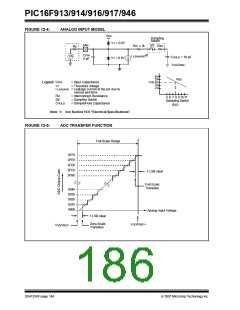
12.3 A/D Acquisition Requirements
For the ADC to meet its specified accuracy, the charge
holding capacitor (CHOLD) must be allowed to fully
charge to the input channel voltage level. The Analog
Input model is shown in Figure 12-4. The source
impedance (RS) and the internal sampling switch (RSS)
impedance directly affect the time required to charge the
capacitor CHOLD. The sampling switch (RSS) impedance
varies over the device voltage (VDD), see Figure 12-4.
The maximum recommended impedance for analog
sources is 10 kΩ. As the source impedance is
decreased, the acquisition time may be decreased.
After the analog input channel is selected (or changed),
EQUATION 12-1: ACQUISITION TIME EXAMPLE
Temperature = 50°C and external impedance of 10kΩ 5.0V VDD
Assumptions:
TACQ = Amplifier Settling Time + Hold Capacitor Charging Time + Temperature Coefficient
= TAMP + TC + TCOFF
= 2μs + TC + [(Temperature - 25°C)(0.05μs/°C)]
The value for TC can be approximated with the following equations:
1
⎛
⎞
;[1] VCHOLD charged to within 1/2 lsb
VAPPLIED 1 – -------------------------- = VCHOLD
(2n + 1) – 1
⎝
⎠
–TC
---------
⎛
⎞
VAPPLIED 1 – e RC = VCHOLD
⎜
⎝
⎟
⎠
;[2] VCHOLD charge response to VAPPLIED
;combining [1] and [2]
–Tc
--------
⎛
⎞
1
VAPPLIED 1 – eRC = VAPPLIED 1 – --------------------------
⎛
⎞
⎠
⎜
⎝
⎟
⎠
(2n + 1) – 1
⎝
Note: Where n = number of bits of the ADC.
Solving for TC:
TC = –CHOLD(RIC + RSS + RS) ln(1/2047)
= –10pF(1kΩ + 7kΩ + 10kΩ) ln(0.0004885)
= 1.37μs
Therefore:
TACQ = 2μS + 1.37μS + [(50°C- 25°C)(0.05μS/°C)]
= 4.67μS
Note 1: The reference voltage (VREF) has no effect on the equation, since it cancels itself out.
2: The charge holding capacitor (CHOLD) is not discharged after each conversion.
3: The maximum recommended impedance for analog sources is 10 kΩ. This is required to meet the pin
leakage specification.
© 2007 Microchip Technology Inc.
DS41250F-page 183

 MICROCHIP [ MICROCHIP ]