PIC16F913/914/916/917/946
12.1.3
ADC VOLTAGE REFERENCE
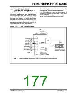
12.1 ADC Configuration
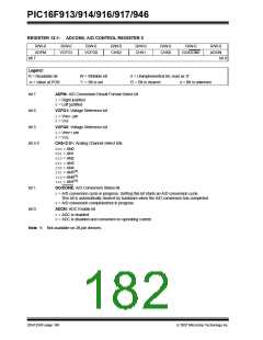
The VCFG bits of the ADCON0 register provide
independent control of the positive and negative
voltage references. The positive voltage reference can
be either VDD or an external voltage source. Likewise,
the negative voltage reference can be either VSS or an
external voltage source.
When configuring and using the ADC the following
functions must be considered:
• Port configuration
• Channel selection
• ADC voltage reference selection
• ADC conversion clock source
• Interrupt control
12.1.4
CONVERSION CLOCK
The source of the conversion clock is software select-
able via the ADCS bits of the ADCON1 register. There
are seven possible clock options:
• Results formatting
12.1.1
PORT CONFIGURATION
• FOSC/2
The ADC can be used to convert both analog and digital
signals. When converting analog signals, the I/O pin
should be configured for analog by setting the associated
TRIS and ANSEL bits. See the corresponding Port
section for more information.
• FOSC/4
• FOSC/8
• FOSC/16
• FOSC/32
Note:
Analog voltages on any pin that is defined
as a digital input may cause the input
buffer to conduct excess current.
• FOSC/64
• FRC (dedicated internal oscillator)
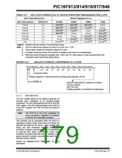
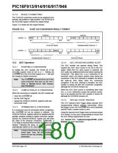
The time to complete one bit conversion is defined as
TAD. One full 10-bit conversion requires 11 TAD periods
as shown in Figure 12-3.
12.1.2
CHANNEL SELECTION
The CHS bits of the ADCON0 register determine which
channel is connected to the sample and hold circuit.
For correct conversion, the appropriate TAD specification
must be met. See A/D conversion requirements in
Section 19.0 “Electrical Specifications” for more
information. Table 12-1 gives examples of appropriate
ADC clock selections.
When changing channels, a delay is required before
starting the next conversion. Refer to Section 12.2
“ADC Operation” for more information.
Note:
Unless using the FRC, any changes in the
system clock frequency will change the
ADC clock frequency, which may
adversely affect the ADC result.
DS41250F-page 176
© 2007 Microchip Technology Inc.

 MICROCHIP [ MICROCHIP ]