PIC16F913/914/916/917/946
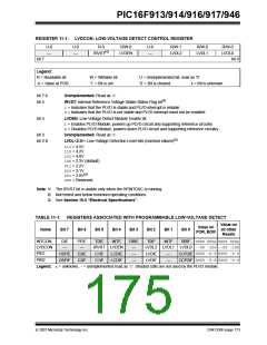
REGISTER 11-1: LVDCON: LOW-VOLTAGE DETECT CONTROL REGISTER
U-0
—
U-0
—
R-0
IRVST(1)
R/W-0
U-0
—
R/W-1
LVDL2
R/W-0
LVDL1
R/W-0
LVDL0
LVDEN
bit 7
bit 0
Legend:
R = Readable bit
-n = Value at POR
W = Writable bit
‘1’ = Bit is set
U = Unimplemented bit, read as ‘0’
‘0’ = Bit is cleared x = Bit is unknown
bit 7-6
bit 5
Unimplemented: Read as ‘0’
IRVST: Internal Reference Voltage Stable Status Flag bit(1)
1= Indicates that the PLVD is stable and PLVD interrupt is reliable
0= Indicates that the PLVD is not stable and PLVD interrupt must not be enabled
bit 4
LVDEN: Low-Voltage Detect Module Enable bit
1= Enables PLVD Module, powers up PLVD circuit and supporting reference circuitry
0= Disables PLVD Module, powers down PLVD circuit and supporting reference circuitry
bit 3
Unimplemented: Read as ‘0’
bit 2-0
LVDL<2:0>: Low-Voltage Detection Level bits (nominal values)(3)
111= 4.5V
110= 4.2V
101= 4.0V
100= 2.3V (default)
011= 2.2V
010= 2.1V
001= 2.0V(2)
000= Reserved
Note 1: The IRVST bit is usable only when the HFINTOSC is running.
2: Not tested and below minimum operating conditions.
3: See Section 19.0 “Electrical Specifications”.
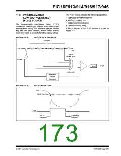
TABLE 11-1: REGISTERS ASSOCIATED WITH PROGRAMMABLE LOW-VOLTAGE DETECT
Value on
all other
Resets
Value on
POR, BOR
Name
Bit 7
Bit 6
Bit 5
Bit 4
Bit 3
Bit 2
Bit 1
Bit 0
INTCON
LVDCON
PIE2
GIE
—
PEIE
—
T0IE
INTE
RBIE
—
T0IF
INTF
RBIF 0000 000x 0000 000x
IRVST LVDEN
LVDL2 LVDL1 LVDL0 --00 -100 --00 -100
0000 -0-0 0000 -0-0
0000 -0-0 0000 -0-0
OSFIE
OSFIF
C2IE
C2IF
C1IE
C1IF
LCDIE
LCDIF
—
LVDIE
LVDIF
—
—
CCP2IE
CCP2IF
PIR2
—
Legend: x= unknown, -= unimplemented read as ‘0’. Shaded cells are not used by the PLVD module.
© 2007 Microchip Technology Inc.
DS41250F-page 173

 MICROCHIP [ MICROCHIP ]