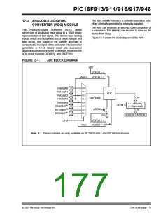
PIC16F913/914/916/917/946
12.1.6
RESULT FORMATTING
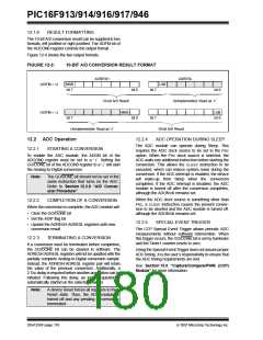
The 10-bit A/D conversion result can be supplied in two
formats, left justified or right justified. The ADFM bit of
the ADCON0 register controls the output format.
Figure 12-4 shows the two output formats.
FIGURE 12-3:
10-BIT A/D CONVERSION RESULT FORMAT
ADRESH
ADRESL
(ADFM = 0)
MSB
bit 7
LSB
bit 0
bit 0
bit 7
bit 7
bit 0
10-bit A/D Result
Unimplemented: Read as ‘0’
(ADFM = 1)
MSB
LSB
bit 0
bit 7
Unimplemented: Read as ‘0’
10-bit A/D Result
12.2.4
ADC OPERATION DURING SLEEP
12.2 ADC Operation
The ADC module can operate during Sleep. This
requires the ADC clock source to be set to the FRC
option. When the FRC clock source is selected, the
ADC waits one additional instruction before starting the
conversion. This allows the SLEEP instruction to be
executed, which can reduce system noise during the
conversion. If the ADC interrupt is enabled, the device
will wake-up from Sleep when the conversion
completes. If the ADC interrupt is disabled, the ADC
module is turned off after the conversion completes,
although the ADON bit remains set.
12.2.1
STARTING A CONVERSION
To enable the ADC module, the ADON bit of the
ADCON0 register must be set to a ‘1’. Setting the
GO/DONE bit of the ADCON0 register to a ‘1’ will start
the Analog-to-Digital conversion.
Note:
The GO/DONE bit should not be set in the
same instruction that turns on the ADC.
Refer to Section 12.2.6 “A/D Conver-
sion Procedure”.
When the ADC clock source is something other than
FRC, a SLEEP instruction causes the present conver-
sion to be aborted and the ADC module is turned off,
although the ADON bit remains set.
12.2.2
COMPLETION OF A CONVERSION
When the conversion is complete, the ADC module will:
• Clear the GO/DONE bit
• Set the ADIF flag bit
12.2.5
SPECIAL EVENT TRIGGER
• Update the ADRESH:ADRESL registers with new
conversion result
The CCP Special Event Trigger allows periodic ADC
measurements without software intervention. When
this trigger occurs, the GO/DONE bit is set by hardware
and the Timer1 counter resets to zero.
12.2.3
TERMINATING A CONVERSION
If a conversion must be terminated before completion,
the GO/DONE bit can be cleared in software. The
ADRESH:ADRESL registers will not be updated with the
partially complete Analog-to-Digital conversion sample.
Instead, the ADRESH:ADRESL register pair will retain
the value of the previous conversion. Additionally, a
2 TAD delay is required before another acquisition can be
initiated. Following this delay, an input acquisition is
automatically started on the selected channel.
Using the Special Event Trigger does not assure proper
ADC timing. It is the user’s responsibility to ensure that
the ADC timing requirements are met.
See Section 15.0 “Capture/Compare/PWM (CCP)
Module” for more information.
Note:
A device Reset forces all registers to their
Reset state. Thus, the ADC module is
turned off and any pending conversion is
terminated.
DS41250F-page 178
© 2007 Microchip Technology Inc.

 MICROCHIP [ MICROCHIP ]