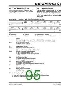
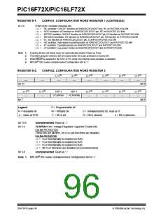
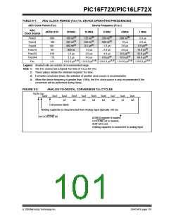
PIC16F72X/PIC16LF72X
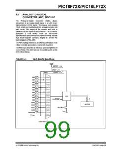
9.0
ANALOG-TO-DIGITAL
CONVERTER (ADC) MODULE
The Analog-to-Digital Converter (ADC) allows
conversion of an analog input signal to a 8-bit binary
representation of that signal. This device uses analog
inputs, which are multiplexed into a single sample and
hold circuit. The output of the sample and hold is
connected to the input of the converter. The converter
generates
a 8-bit binary result via successive
approximation and stores the conversion result into the
ADC result register (ADRES). Figure 9-1 shows the
block diagram of the ADC.
The ADC voltage reference is software selectable to be
either internally generated or externally supplied.
The ADC can generate an interrupt upon completion of
a conversion. This interrupt can be used to wake-up the
device from Sleep.
FIGURE 9-1:
ADC BLOCK DIAGRAM
AVDD
ADREF = 0x
ADREF = 11
VREF+
ADREF = 10
0000
AN0
AN1
0001
0010
0011
0100
0101
AN2
AN3
AN4
AN5
0110
0111
1000
1001
1010
1011
1100
1101
1110
1111
AN6
AN7
ADC
AN8
8
GO/DONE
ADON
AN9
AN10
AN11
AN12
AN13
Reserved
FVREF
ADRES
VSS
CHS<3:0>
© 2009 Microchip Technology Inc.
DS41341E-page 99

 MICROCHIP [ MICROCHIP ]