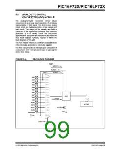
PIC16F72X/PIC16LF72X
9.1.5
INTERRUPTS
9.2.3
TERMINATING A CONVERSION
The ADC module allows for the ability to generate an
interrupt upon completion of an Analog-to-Digital
conversion. The ADC interrupt flag is the ADIF bit in the
PIR1 register. The ADC interrupt enable is the ADIE bit
in the PIE1 register. The ADIF bit must be cleared in
software.
If a conversion must be terminated before completion,
the GO/DONE bit can be cleared in software. The
ADRES register will be updated with the partially com-
plete Analog-to-Digital conversion sample. Incomplete
bits will match the last bit converted.
Note:
A device Reset forces all registers to their
Reset state. Thus, the ADC module is
turned off and any pending conversion is
terminated.
Note 1: The ADIF bit is set at the completion of
every conversion, regardless of whether
or not the ADC interrupt is enabled.
2: The ADC operates during Sleep only
9.2.4
ADC OPERATION DURING SLEEP
when the FRC oscillator is selected.
The ADC module can operate during Sleep. This
requires the ADC clock source to be set to the FRC
option. When the FRC clock source is selected, the
ADC waits one additional instruction before starting the
conversion. This allows the SLEEP instruction to be
executed, which can reduce system noise during the
conversion. If the ADC interrupt is enabled, the device
will wake-up from Sleep when the conversion
completes. If the ADC interrupt is disabled, the ADC
module is turned off after the conversion completes,
although the ADON bit remains set.
This interrupt can be generated while the device is
operating or while in Sleep. If the device is in Sleep, the
interrupt will wake-up the device. Upon waking from
Sleep, the next instruction following the SLEEPinstruc-
tion is always executed. If the user is attempting to
wake-up from Sleep and resume in-line code execu-
tion, the GIE and PEIE bits of the INTCON register
must be disabled. If the GIE and PEIE bits of the INT-
CON register are enabled, execution will switch to the
Interrupt Service Routine.
Please refer to Section 9.1.5 “Interrupts” for more
information.
When the ADC clock source is something other than
FRC, a SLEEP instruction causes the present conver-
sion to be aborted and the ADC module is turned off,
although the ADON bit remains set.
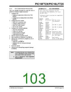
9.2
ADC Operation
9.2.1
STARTING A CONVERSION
9.2.5
SPECIAL EVENT TRIGGER
To enable the ADC module, the ADON bit of the
ADCON0 register must be set to a ‘1’. Setting the GO/
DONE bit of the ADCON0 register to a ‘1’ will start the
Analog-to-Digital conversion.
The Special Event Trigger of the CCP module allows
periodic ADC measurements without software inter-
vention. When this trigger occurs, the GO/DONE bit is
set by hardware and the Timer1 counter resets to zero.
Note:
The GO/DONE bit should not be set in the
same instruction that turns on the ADC.
Refer to Section 9.2.6 “A/D Conversion
Procedure”.
Using the Special Event Trigger does not assure proper
ADC timing. It is the user’s responsibility to ensure that
the ADC timing requirements are met.
Refer to Section 15.0 “Capture/Compare/PWM
(CCP) Module” for more information.
9.2.2
COMPLETION OF A CONVERSION
When the conversion is complete, the ADC module will:
• Clear the GO/DONE bit
• Set the ADIF Interrupt Flag bit
• Update the ADRES register with new conversion
result
DS41341E-page 102
© 2009 Microchip Technology Inc.

 MICROCHIP [ MICROCHIP ]