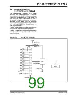
PIC16F72X/PIC16LF72X
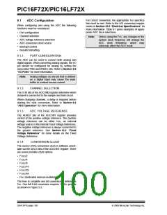
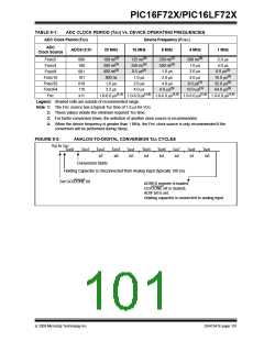
TABLE 9-1:
ADC CLOCK PERIOD (TAD) VS. DEVICE OPERATING FREQUENCIES
ADC Clock Period (TAD)
Device Frequency (FOSC)
ADC
Clock Source
ADCS<2:0>
20 MHz
16 MHz
8 MHz
4 MHz
1 MHz
Fosc/2
Fosc/4
Fosc/8
Fosc/16
Fosc/32
Fosc/64
FRC
000
100
001
101
010
110
x11
100 ns(2)
200 ns(2)
400 ns(2)
800 ns
125 ns(2)
250 ns(2)
0.5 μs(2)
1.0 μs
250 ns(2)
500 ns(2)
1.0 μs
500 ns(2)
1.0 μs
2.0 μs
4.0 μs
8.0 μs(3)
16.0 μs(3)
32.0 μs(3)
64.0 μs(3)
2.0 μs
2.0 μs
4.0 μs
1.6 μs
2.0 μs
4.0 μs
8.0 μs(3)
8.0 μs(3)
16.0 μs(3)
3.2 μs
4.0 μs
1.0-6.0 μs(1,4) 1.0-6.0 μs(1,4) 1.0-6.0 μs(1,4) 1.0-6.0 μs(1,4) 1.0-6.0 μs(1,4)
Legend: Shaded cells are outside of recommended range.
Note 1: The FRC source has a typical TAD time of 1.6 μs for VDD.
2: These values violate the minimum required TAD time.
3: For faster conversion times, the selection of another clock source is recommended.
4: When the device frequency is greater than 1 MHz, the FRC clock source is only recommended if the
conversion will be performed during Sleep.
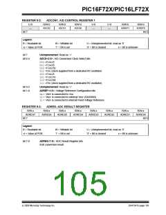
FIGURE 9-2:
ANALOG-TO-DIGITAL CONVERSION TAD CYCLES
Tcy to TAD
TAD0
TAD1
TAD2
b7
TAD3
b6
TAD4
TAD5
b4
TAD6
b3
TAD7
TAD8
TAD9
b5
b2
b1
b0
Conversion Starts
Holding Capacitor is Disconnected from Analog Input (typically 100 ns)
Set GO/DONE bit
ADRES register is loaded,
GO/DONE bit is cleared,
ADIF bit is set,
Holding capacitor is connected to analog input
© 2009 Microchip Technology Inc.
DS41341E-page 101

 MICROCHIP [ MICROCHIP ]