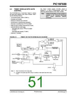
PIC16F688
6.5
Timer1 Operation in
Asynchronous Counter Mode
6.6
Timer1 Oscillator
A crystal oscillator circuit is built-in between pins OSC1
(input) and OSC2 (amplifier output). It is enabled by
setting control bit, T1OSCEN (T1CON<3>). The oscil-
lator is a low power oscillator rated up to 32 kHz. It will
continue to run during Sleep. It is primarily intended for
a 32 kHz crystal. Table 3-1 shows the capacitor selec-
tion for the Timer1 oscillator.
If control bit T1SYNC (T1CON<2>) is set, the external
clock input is not synchronized. The timer continues to
increment asynchronous to the internal phase clocks.
The timer will continue to run during Sleep and can
generate an interrupt-on-overflow, which will wake-up
the processor. However, special precautions in
software are needed to read/write the timer (see
Section 6.5.1 “Reading and Writing Timer1 in
Asynchronous Counter Mode”).
The Timer1 oscillator is shared with the system LP
oscillator. Thus, Timer1 can use this mode only when
the primary system clock is derived from the internal
oscillator. As with the system LP oscillator, the user
must provide a software time delay to ensure proper
oscillator start-up.
Note: The ANSEL (91h) and CMCON0 (19h)
registers must be initialized to configure an
analog channel as a digital input. Pins
configured as analog inputs will read ‘0’.
TRISA5 and TRISA4 bits are set when the Timer1
oscillator is enabled. RA5 and RA4 read as ‘0’ and
TRISA5 and TRISA4 bits read as ‘1’.
6.5.1
READING AND WRITING TIMER1 IN
ASYNCHRONOUS COUNTER
MODE
Note: The oscillator requires a start-up and
stabilization time before use. Thus,
T1OSCEN should be set and a suitable
delay observed prior to enabling Timer1.
Reading TMR1H or TMR1L, while the timer is running
from an external asynchronous clock, will ensure a
valid read (taken care of in hardware). However, the
user should keep in mind that reading the 16-bit timer
in two 8-bit values itself, poses certain problems, since
the timer may overflow between the reads.
6.7
Timer1 Operation During Sleep
Timer1 can only operate during Sleep when setup in
Asynchronous Counter mode. In this mode, an external
crystal or clock source can be used to increment the
counter. To set up the timer to wake the device:
For writes, it is recommended that the user simply stop
the timer and write the desired values. A write conten-
tion may occur by writing to the timer registers, while
the register is incrementing. This may produce an
unpredictable value in the timer register.
• Timer1 must be on (T1CON<0>)
• TMR1IE bit (PIE1<0>) must be set
• PEIE bit (INTCON<6>) must be set
Reading the 16-bit value requires some care.
Examples in the “PICmicro® Mid-Range MCU Family
Reference Manual” (DS33023) show how to read and
write Timer1 when it is running in Asynchronous mode.
The device will wake-up on an overflow. If the GIE bit
(INTCON<7>) is set, the device will wake-up and jump
to the Interrupt Service Routine (0004h) on an overflow.
If the GIE bit is clear, execution will continue with the
next instruction.
TABLE 6-1:
REGISTERS ASSOCIATED WITH TIMER1
Value on
Value on
POR, BOD
Addr
Name
Bit 7
Bit 6
Bit 5
Bit 4
Bit 3
Bit 2
Bit 1
Bit 0
all other
Resets
0Bh/
8Bh
INTCON
GIE
PEIE
ADIF
T0IE
INTE
C2IF
RAIE
C1IF
T0IF
INTF
TXIF
RAIF
0000 0000 0000 0000
0Ch
0Eh
0Fh
10h
1Ah
8Ch
PIR1
EEIF
RCIF
OSFIF
TMR1IF 0000 0000 0000 0000
xxxx xxxx uuuu uuuu
TMR1L
Holding register for the Least Significant Byte of the 16-bit TMR1 register
TMR1H Holding register for the Most Significant Byte of the 16-bit TMR1 register
xxxx xxxx uuuu uuuu
T1CON
CMCON1
PIE1
T1GINV TMR1GE T1CKPS1 T1CKPS0 T1OSCEN T1SYNC TMR1CS TMR1ON 0000 0000 uuuu uuuu
—
—
—
—
—
—
T1GSS C2SYNC ---- --10 ---- --10
TXIE TMR1IE 0000 0000 0000 0000
EEIE
ADIE
RCIE
C2IE
C1IE
OSFIE
Legend: x= unknown, u= unchanged, - = unimplemented, read as ‘0’. Shaded cells are not used by the Timer1 module.
DS41203B-page 52
Preliminary
2004 Microchip Technology Inc.

 MICROCHIP [ MICROCHIP ]