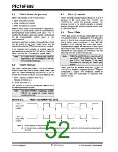
PIC16F688
7.1
Comparator Operation
7.2
Analog Input Connection
Considerations
A single comparator is shown in Figure 7-1 along with
the relationship between the analog input levels and
the digital output. When the analog input at VIN+ is less
than the analog input VIN-, the output of the comparator
is a digital low level. When the analog input at VIN+ is
greater than the analog input VIN-, the output of the
comparator is a digital high level. The shaded areas of
the output of the comparator in Figure 7-1 represent
the uncertainty due to input offsets and response time.
A simplified circuit for an analog input is shown in
Figure 7-2. Since the analog pins are connected to a
digital output, they have reverse biased diodes to VDD
and VSS. The analog input, therefore, must be between
VSS and VDD. If the input voltage deviates from this
range by more than 0.6V in either direction, one of the
diodes is forward biased and a latch-up may occur. A
maximum source impedance of 10 kΩ is recommended
for the analog sources. Any external component
connected to an analog input pin, such as a capacitor
or a Zener diode, should have very little leakage
current.
Note: To use CIN+ and CIN- pins as analog
inputs, the appropriate bits must be
programmed in the CMCON0 (19h)
register.
Note 1: When reading the PORT register, all pins
configured as analog inputs will read as a
‘0’. Pins configured as digital inputs will
convert as analog inputs according to the
input specification.
The polarity of the comparator output can be inverted
by setting the CxINV bits (CMCON0<5:4>). Clearing
CxINV results in a non-inverted output. A complete
table showing the output state versus input conditions
and the polarity bit is shown in Table 7-1.
2: Analog levels on any pin defined as a
digital input may cause the input buffer to
consume more current than is specified.
TABLE 7-1:
OUTPUT STATE VS. INPUT
CONDITIONS
Input Conditions
CINV
CxOUT
VIN- > VIN+
VIN- < VIN+
VIN- > VIN+
VIN- < VIN+
0
0
1
1
0
1
1
0
FIGURE 7-1:
SINGLE COMPARATOR
VIN+
VIN-
+
Output
–
VIN-
V
IN–
VIN+
V
IN+
Output
Output
DS41203B-page 54
Preliminary
2004 Microchip Technology Inc.

 MICROCHIP [ MICROCHIP ]