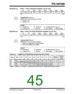
PIC16F688
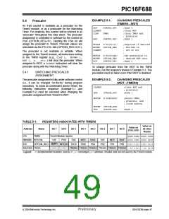
EXAMPLE 5-1:
CHANGING PRESCALER
(TIMER0→WDT)
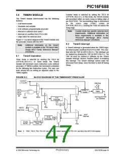
5.4
Prescaler
An 8-bit counter is available as a prescaler for the
Timer0 module, or as a postscaler for the Watchdog
Timer. For simplicity, this counter will be referred to as
“prescaler” throughout this data sheet. The prescaler
assignment is controlled in software by the control bit
PSA (OPTION_REG<3>). Clearing the PSA bit will
assign the prescaler to Timer0. Prescale values are
selectable via the PS<2:0> bits (OPTION_REG<2:0>).
BCF
STATUS,RP0
;Bank 0
CLRWDT
CLRF
;Clear WDT
;Clear TMR0 and
; prescaler
;Bank 1
TMR0
BSF
STATUS,RP0
MOVLW
MOVWF
CLRWDT
b’00101111’
OPTION_REG
;Required if desired
; PS2:PS0 is
; 000 or 001
;
;Set postscaler to
; desired WDT rate
;Bank 0
The prescaler is not readable or writable. When
assigned to the Timer0 module, all instructions writing
to the TMR0 register (e.g., CLRF 1, MOVWF 1,
BSF 1, x....etc.) will clear the prescaler. When
assigned to WDT, a CLRWDT instruction will clear the
prescaler along with the Watchdog Timer.
MOVLW
MOVWF
BCF
b’00101xxx’
OPTION_REG
STATUS,RP0
To change prescaler from the WDT to the TMR0
module, use the sequence shown in Example 5-2. This
precaution must be taken even if the WDT is disabled.
5.4.1
SWITCHING PRESCALER
ASSIGNMENT
EXAMPLE 5-2:
CHANGING PRESCALER
(WDT→TIMER0)
The prescaler assignment is fully under software control
(i.e., it can be changed “on-the-fly” during program
execution). To avoid an unintended device Reset, the
following instruction sequence (Example 5-1 and
Example 5-2) must be executed when changing the
prescaler assignment from Timer0 to WDT.
CLRWDT
;Clear WDT and
; prescaler
;Bank 1
BSF
STATUS,RP0
b’xxxx0xxx’
MOVLW
;Select TMR0,
; prescale, and
; clock source
;
MOVWF
BCF
OPTION_REG
STATUS,RP0
;Bank 0
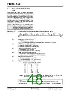
TABLE 5-1:
REGISTERS ASSOCIATED WITH TIMER0
Value on
all other
Resets
Value on
POR, BOD
Address
Name
Bit 7
Bit 6
Bit 5
Bit 4
Bit 3
Bit 2
Bit 1
Bit 0
01h
0Bh/8Bh INTCON
81h OPTION_REG RAPU INTEDG T0CS
85h/185h TRISA
Legend: - = Unimplemented locations, read as ‘0’, u= unchanged, x= unknown. Shaded cells are not used by the Timer0 module.
TMR0
Timer0 Module register
xxxx xxxx uuuu uuuu
RAIF 0000 0000 0000 0000
PS0 1111 1111 1111 1111
GIE PEIE T0IE
INTE
RAIE
PSA
T0IF
PS2
INTF
PS1
T0SE
—
—
TRISA5 TRISA4 TRISA3 TRISA2 TRISA1 TRISA0 --11 1111 --11 1111
2004 Microchip Technology Inc.
Preliminary
DS41203B-page 47

 MICROCHIP [ MICROCHIP ]