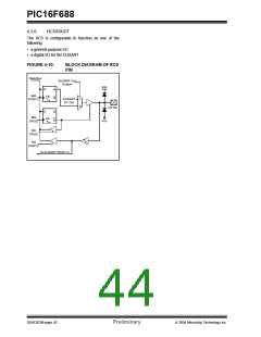
PIC16F688
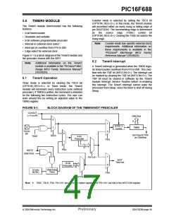
5.3
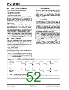
Using Timer0 with an External
Clock
When no prescaler is used, the external clock input is
the same as the prescaler output. The synchronization
of T0CKI, with the internal phase clocks, is accom-
plished by sampling the prescaler output on the Q2 and
Q4 cycles of the internal phase clocks. Therefore, it is
necessary for T0CKI to be high for at least 2 TOSC (and
a small RC delay of 20 ns) and low for at least 2 TOSC
(and a small RC delay of 20 ns). Refer to the electrical
specification of the desired device.
Note:
The ANSEL (91h) and CMCON0 (19h)
registers must be initialized to configure
an analog channel as a digital input. Pins
configured as analog inputs will read ‘0’.
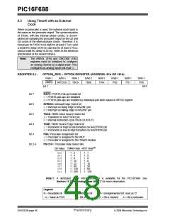
REGISTER 5-1:
OPTION_REG – OPTION REGISTER (ADDRESS: 81h OR 181h)
R/W-1
RAPU
R/W-1
R/W-1
T0CS
R/W-1
T0SE
R/W-1
PSA
R/W-1
PS2
R/W-1
PS1
R/W-1
PS0
INTEDG
bit 7
bit 0
bit 7
bit 6
bit 5
bit 4
bit 3
bit 2-0
RAPU: PORTA Pull-up Enable bit
1= PORTA pull-ups are disabled
0= PORTA pull-ups are enabled by individual port latch values in WPUA register
INTEDG: Interrupt Edge Select bit
1= Interrupt on rising edge of RA2/INT pin
0= Interrupt on falling edge of RA2/INT pin
T0CS: TMR0 Clock Source Select bit
1= Transition on RA2/T0CKI pin
0= Internal instruction cycle clock (CLKOUT)
T0SE: TMR0 Source Edge Select bit
1= Increment on high-to-low transition on RA2/T0CKI pin
0= Increment on low-to-high transition on RA2/T0CKI pin
PSA: Prescaler Assignment bit
1= Prescaler is assigned to the WDT
0= Prescaler is assigned to the Timer0 module
PS<2:0>: Prescaler Rate Select bits
Bit Value TMR0 Rate WDT Rate(1)
000
001
010
011
100
101
110
111
1 : 2
1 : 1
1 : 2
1 : 4
1 : 8
1 : 16
1 : 32
1 : 64
1 : 128
1 : 4
1 : 8
1 : 16
1 : 32
1 : 64
1 : 128
1 : 256
Note 1: A dedicated 16-bit WDT postscaler is available for the PIC16F688. See
Section 11.7 “Watchdog Timer (WDT)” for more information.
Legend:
R = Readable bit
W = Writable bit
‘1’ = Bit is set
U = Unimplemented bit, read as ‘0’
‘0’ = Bit is cleared x = Bit is unknown
- n = Value at POR
DS41203B-page 46
Preliminary
2004 Microchip Technology Inc.

 MICROCHIP [ MICROCHIP ]