PIC12F508/509/16F505
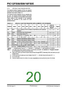
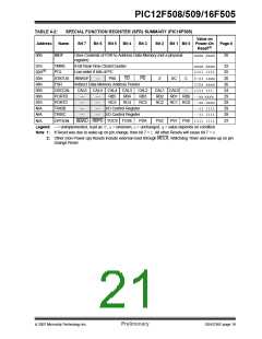
TABLE 4-2:
Address
SPECIAL FUNCTION REGISTER (SFR) SUMMARY (PIC16F505)
Value on
Bit 1 Bit 0 Power-On
Reset(2)
Name
INDF
TMR0
Bit 7
Bit 6
Bit 5
Bit 4
Bit 3
Bit 2
Page #
00h
Uses Contents of FSR to Address Data Memory (not a physical
register)
xxxx xxxx
26
01h
02h(1)
03h
04h
05h
06h
07h
N/A
N/A
N/A
8-bit Real-Time Clock/Counter
Low-order 8 bits of PC
xxxx xxxx
1111 1111
0-01 1xxx
110x xxxx
1111 111-
33
25
20
26
24
29
29
29
29
23
PCL
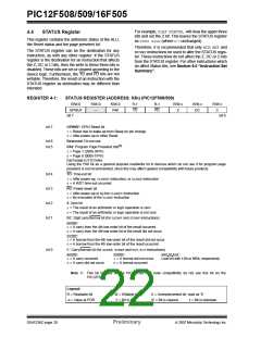
STATUS
FSR
RBWUF
—
PA0
TO
PD
Z
DC
C
Indirect Data Memory Address Pointer
OSCCAL
PORTB
PORTC
TRISB
TRISC
OPTION
CAL6
—
CAL5 CAL4 CAL3
CAL2
RB3
CAL1 CAL0
—
—
—
—
—
RB5
RC5
RB4
RC4
RB2
RC2
RB1 RB0 --xxxxxx
RC1 RC0 --xx xxxx
--11 1111
—
RC3
—
I/O Control Register
I/O Control Register
—
--11 1111
RBWU RBPU TOCS TOSE
PSA
PS2
PS1 PS0 1111 1111
Legend: – = unimplemented, read as ‘0’, x= unknown, u= unchanged, q= value depends on condition.
Note 1: If Reset was due to wake-up on pin change, then bit 7 = 1. All other Resets will cause bit 7 = 0.
2: Other (non Power-up) Resets include external reset through MCLR, Watchdog Timer and wake-up on pin
change Reset.
© 2007 Microchip Technology Inc.
Preliminary
DS41236C-page 19

 MICROCHIP [ MICROCHIP ]