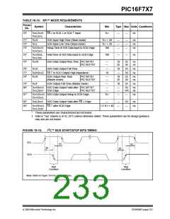
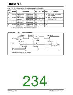
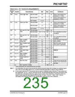
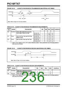
PIC16F7X7
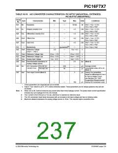
TABLE 18-15: A/D CONVERTER CHARACTERISTICS: PIC16F7X7 (INDUSTRIAL, EXTENDED)
PIC16LF7X7 (INDUSTRIAL)
Param
No.
Sym
NR
Characteristic
Resolution
Min
Typ†
Max
Units
Conditions
A01
—
—
10 bits
bit VREF = VDD = 5.12V,
VSS ≤ VAIN ≤ VREF
A03
A04
A06
A07
EIL
Integral Linearity Error
—
—
—
—
—
—
—
—
<±1
<±1
<±2
<±1
LSb VREF = VDD = 5.12V,
VSS ≤ VAIN ≤ VREF
EDL
Differential Linearity Error
LSb VREF = VDD = 5.12V,
VSS ≤ VAIN ≤ VREF
EOFF Offset Error
LSb VREF = VDD = 5.12V,
VSS ≤ VAIN ≤ VREF
EGN
Gain Error
LSb VREF = VDD = 5.12V,
VSS ≤ VAIN ≤ VREF
(3)
A10
A20
—
Monotonicity
—
guaranteed
—
—
—
V
VSS ≤ VAIN ≤ VREF
VREF Reference Voltage
(VREF+ – VREF-)
2.0
VDD + 0.3
A21
A22
A25
A30
VREF+ Reference Voltage High
VREF- Reference Voltage Low
AVDD – 2.5V
AVSS – 0.3V
VSS – 0.3V
—
—
—
—
—
AVDD + 0.3V
VREF+ – 2.0V
VREF + 0.3V
2.5
V
V
V
VAIN
ZAIN
Analog Input Voltage
Recommended Impedance of
Analog Voltage Source
kΩ (Note 4)
A40
A50
IAD
A/D Conversion PIC16F7X7
—
—
220
90
—
—
µA Average current
Current (VDD)
consumption when A/D is on
(Note 1)
PIC16LF7X7
µA
IREF
VREF Input Current (Note 2)
—
—
5
µA During VAIN acquisition.
Based on differential of VHOLD
to VAIN to charge CHOLD,
see Section 12.1 “A/D
Acquisition Requirements”.
µA During A/D conversion cycle
—
—
150
*
These parameters are characterized but not tested.
†
Data in “Typ” column is at 5V, 25°C unless otherwise stated. These parameters are for design guidance only and are
not tested.
Note 1: When A/D is off, it will not consume any current other than minor leakage current. The power-down current specification
includes any such leakage from the A/D module.
2: VREF current is from RA3 pin or VDD pin, whichever is selected as reference input.
3: The A/D conversion result never decreases with an increase in the input voltage and has no missing codes.
4: Maximum allowed impedance for analog voltage source is 10 kΩ. This requires higher acquisition time.
2004 Microchip Technology Inc.
DS30498C-page 235

 MICROCHIP [ MICROCHIP ]