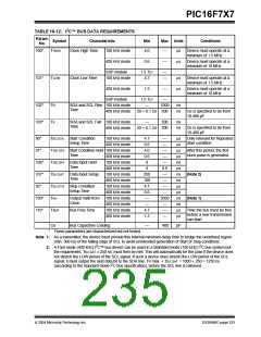
PIC16F7X7
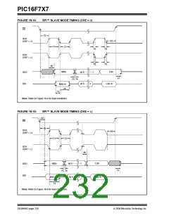
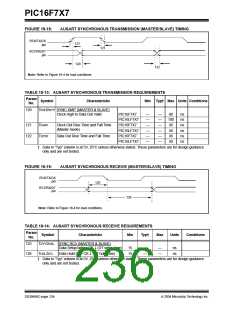
FIGURE 18-18:
AUSART SYNCHRONOUS TRANSMISSION (MASTER/SLAVE) TIMING
RC6/TX/CK
pin
121
121
RC7/RX/DT
pin
120
122
Note: Refer to Figure 18-4 for load conditions.
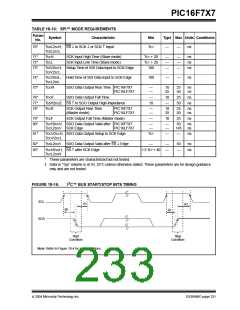
TABLE 18-13: AUSART SYNCHRONOUS TRANSMISSION REQUIREMENTS
Param
Symbol
Characteristic
Min Typ† Max Units Conditions
No.
120
TCKH2DTV SYNC XMIT (MASTER & SLAVE)
Clock High to Data Out Valid
PIC16F7X7
PIC16LF7X7
PIC16F7X7
PIC16LF7X7
PIC16F7X7
PIC16LF7X7
—
—
—
—
—
—
—
—
—
—
—
—
80
100
45
ns
ns
ns
ns
ns
ns
121
122
TCKRF
TDTRF
Clock Out Rise Time and Fall Time
(Master mode)
50
Data Out Rise Time and Fall Time
45
50
†
Data in “Typ” column is at 5V, 25°C unless otherwise stated. These parameters are for design guidance
only and are not tested.
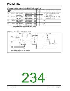
FIGURE 18-19:
AUSART SYNCHRONOUS RECEIVE (MASTER/SLAVE) TIMING
RC6/TX/CK
pin
125
RC7/RX/DT
pin
126
Note: Refer to Figure 18-4 for load conditions.
TABLE 18-14: AUSART SYNCHRONOUS RECEIVE REQUIREMENTS
Param
Symbol
Characteristic
Min
Typ†
Max
Units
Conditions
No.
125
TDTV2CKL SYNC RCV (MASTER & SLAVE)
Data Setup before CK ↓ (DT setup time)
15
15
—
—
—
—
ns
ns
126
TCKL2DTL
Data Hold after CK ↓ (DT hold time)
†
Data in “Typ” column is at 5V, 25°C unless otherwise stated. These parameters are for design guidance
only and are not tested.
DS30498C-page 234
2004 Microchip Technology Inc.

 MICROCHIP [ MICROCHIP ]