PIC16C55X(A)
Plastic Small Outline Family
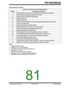
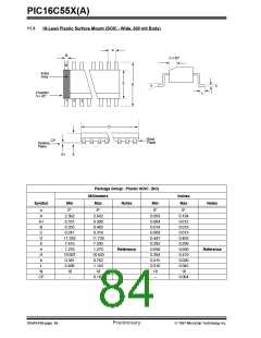
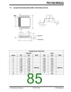
Symbol
Symbol List for Small Outline Package Parameters
Description of Parameters
α
A
Angular spacing between min. and max. lead positions measured at the gauge plane
Distance between seating plane to highest point of body
Distance between seating plane and base plane
Width of terminals
A1
B
C
D
E
Thickness of terminals
Largest overall package parameter of length
Largest overall package width parameter not including leads
Linear spacing of true minimum lead position center line to center line
Largest overall package dimension of width
Length of terminal for soldering to a substrate
Total number of potentially usable lead positions
Seating plane coplanarity
e
H
L
N
CP
Notes:
1. Controlling parameter: inches.
2. All packages are gull wing lead form.
3. "D" and "E" are reference datums and do not include mold flash or protrusions. Mold flash or protrusions shall
not exceed .006 package ends and .010 on sides.
4. The chamfer on the body is optional. If it is not present, a visual index feature must be located within the
cross-hatched area to indicate pin 1 position.
5. Terminal numbers are shown for reference.
1997 Microchip Technology Inc.
Preliminary
DS40143B-page 83

 MICROCHIP [ MICROCHIP ]