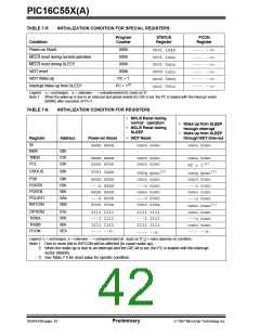
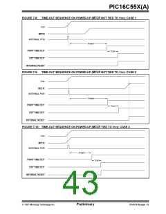
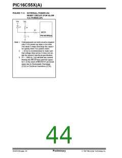
PIC16C55X(A)
7.5.1
RB0/INT INTERRUPT
7.5.2
TMR0 INTERRUPT
An external interrupt on RB0/INT pin is edge triggered:
either rising if INTEDG bit (OPTION<6>) is set, or fall-
ing if INTEDG bit is clear. When a valid edge appears
on the RB0/INT pin, the INTF bit (INTCON<1>) is set.
This interrupt can be disabled by clearing the INTE
control bit (INTCON<4>).The INTF bit must be cleared
in software in the interrupt service routine before
re-enabling this interrupt. The RB0/INT interrupt can
wake-up the processor from SLEEP, if the INTE bit was
set prior to going into SLEEP. The status of the GIE bit
decides whether or not the processor branches to the
interrupt vector following wake-up. See Section 7.8 for
details on SLEEP and Figure 7-16 for timing of
wake-up from SLEEP through RB0/INT interrupt.
An overflow (FFh → 00h) in the TMR0 register will
set the T0IF (INTCON<2>) bit. The interrupt can
be enabled/disabled by setting/clearing T0IE
(INTCON<5>) bit. For operation of the Timer0 module,
see Section 6.0.
7.5.3
PORTB INTERRUPT
An input change on PORTB <7:4> sets the RBIF
(INTCON<0>) bit. The interrupt can be enabled/dis-
abled by setting/clearing the RBIE (INTCON<4>) bit.
For operation of PORTB (Section 5.2).
Note: If a change on the I/O pin should occur
when the read operation is being executed
(start of the Q2 cycle), then the RBIF inter-
rupt flag may get set.
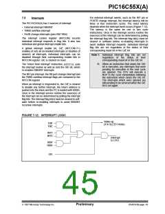
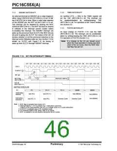
FIGURE 7-13: INT PIN INTERRUPT TIMING
Q1 Q2 Q3 Q4 Q1 Q2 Q3 Q4 Q1 Q2 Q3 Q4 Q1 Q2 Q3 Q4 Q1 Q2 Q3 Q4
OSC1
CLKOUT
3
4
INT pin
1
1
Interrupt Latency
INTF flag
(INTCON<1>)
5
2
GIE bit
(INTCON<7>)
INSTRUCTION FLOW
PC
PC
PC+1
PC+1
—
0004h
0005h
Instruction
fetched
Inst (PC+1)
Inst (0004h)
Inst (PC)
Inst (0005h)
Inst (0004h)
Instruction
executed
Dummy Cycle
Dummy Cycle
Inst (PC)
Inst (PC-1)
Note
1: INTF flag is sampled here (every Q1).
2: Interrupt latency = 3-4 Tcy where Tcy = instruction cycle time.
Latency is the same whether Inst (PC) is a single cycle or a 2-cycle instruction.
3: CLKOUT is available only in RC oscillator mode.
4: For minimum width of INT pulse, refer to AC specs.
5: INTF is enabled to be set anytime during the Q4-Q1 cycles.
DS40143B-page 46
Preliminary
1997 Microchip Technology Inc.

 MICROCHIP [ MICROCHIP ]