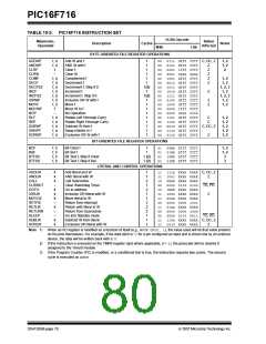
PIC16F716
WDT time-out period values may be found in the
Electrical Specifications section under TWDT (parameter
#31). Values for the WDT prescaler (actually a
postscaler, but shared with the Timer0 prescaler) may be
assigned using the OPTION register.
9.12 Watchdog Timer (WDT)
The Watchdog Timer is a free running, on-chip, RC
oscillator which does not require any external
components. This RC oscillator is separate from the RC
oscillator of the OSC1/CLKIN pin. That means that the
WDT will run, even if the clock on the OSC1/CLKIN and
OSC2/CLKOUT pins of the device have been stopped,
for example, by execution of a SLEEPinstruction.
Note:
The CLRWDTand SLEEPinstructions clear
the WDT and the postscaler, if assigned to
the WDT, and prevent it from timing out
and generating a device Reset condition.
During normal operation, a WDT time-out generates a
device Reset (Watchdog Timer Reset). If the device is in
Sleep mode, a WDT time-out causes the device to
wake-up and continue with normal operation (Watchdog
Timer Wake-up). The TO bit in the STATUS register will
be cleared upon a Watchdog Timer time-out.
.
Note:
When a CLRWDT instruction is executed
and the prescaler is assigned to the WDT,
the prescaler count will be cleared, but the
prescaler assignment is not changed.
The WDT can be permanently disabled by clearing
Configuration bit WDTE (Section 9.1 “Configuration
Bits”).
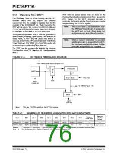
FIGURE 9-14:
WATCHDOG TIMER BLOCK DIAGRAM
From TMR0 Clock Source (Figure 4-1)
0
Postscaler
M
1
U
WDT Timer
X
8
8-to-1 MUX
PS2:PS0
PSA
WDT
Enable Bit
To TMR0 (Figure 4-1)
0
1
MUX
PSA
WDT
Time-out
Note:
PSA and PS2:PS0 are bits in the OPTION register.
TABLE 9-7:
SUMMARY OF REGISTERS ASSOCIATED WITH WATCHDOG TIMER
Value on
all other
Resets
Value on
POR, BOR
Name
Bit 7
Bit 6
Bit 5
Bit 4
Bit 3
Bit 2
Bit 1
Bit 0
CONFIG1(1)
BORV
RBPU
BOREN
INTEDG
—
—
PWRTE
PSA
WDTE
PS2
FOSC1
PS1
FOSC0
PS0
—
—
OPTION_REG
T0CS
T0SE
1111 1111
1111 1111
Legend:
x= unknown, u= unchanged, -= unimplemented locations read as ‘0’. Shaded cells are not used the Watchdog Timer.
Note 1:
See Configuration Word Register (Register 9-1) for operation of all register bits.
DS41206B-page 74
© 2007 Microchip Technology Inc.

 MICROCHIP [ MICROCHIP ]