PIC16F716
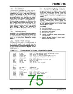
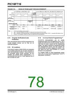
FIGURE 9-15:
WAKE-UP FROM SLEEP THROUGH INTERRUPT
Q1 Q2 Q3 Q4 Q1 Q2 Q3 Q4 Q1
Q1 Q2 Q3 Q4 Q1 Q2 Q3 Q4 Q1 Q2 Q3 Q4 Q1 Q2 Q3 Q4
OSC1
CLKOUT(4)
INT pin
TOST(2)
INTF flag
Interrupt Latency
(INTCON Reg.)
(Note 3)
GIE bit
Processor in
Sleep
(INTCON Reg.)
INSTRUCTION FLOW
PC
PC
PC+1
PC+2
PC+2
PC + 2
0004h
0005h
Instruction
Inst(0004h)
Inst(PC + 1)
Inst(PC + 2)
Inst(0005h)
Inst(PC) = Sleep
fetched
Instruction
executed
Dummy cycle
Dummy cycle
Sleep
Inst(PC + 1)
Inst(PC - 1)
Inst(0004h)
Note 1:
XT, HS or LP Oscillator mode assumed.
TOST = 1024TOSC (drawing not to scale). This delay will not be there for RC Osc mode.
GIE = 1assumed. In this case after wake- up, the processor jumps to the interrupt routine. If GIE = 0, execution will continue in-line.
2:
3:
4:
CLKOUT is not available in these osc modes, but shown here for timing reference.
9.14 Program Verification/Code
Protection
9.16
In-Circuit Serial Programming™
PIC16F716
microcontrollers
can
be
serially
programmed while in the end application circuit. This is
simply done with two lines for clock and data, and three
other lines for power, ground and the programming
voltage. This allows customers to manufacture boards
with unprogrammed devices and then program the
microcontroller just before shipping the product. This
also allows the most recent firmware or a custom
firmware to be programmed.
If the code protection bit has not been programmed, the
on-chip program memory can be read out for
verification purposes.
9.15 ID Locations
Four memory locations (2000h-2003h) are designated
as ID locations where the user can store checksum or
other code-identification numbers. These locations are
not accessible during normal execution, but are
readable and writable during program/verify. It is
recommended that only the 4 Least Significant bits of
the ID location are used.
For complete details on serial programming, please
refer to the In-Circuit Serial Programming™ (ICSP™)
Specification, (DS40245).
DS41206B-page 76
© 2007 Microchip Technology Inc.

 MICROCHIP [ MICROCHIP ]