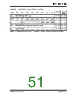
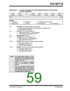
PIC16F716
8.3.1
PWM PERIOD
8.3.2
PWM DUTY CYCLE
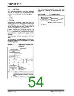
The PWM period is specified by the PR2 register of
Timer2. The PWM period can be calculated using the
formula of Equation 8-1.
The PWM duty cycle is specified by writing a 10-bit
value to multiple registers: CCPR1L register and
DC1B<1:0> bits of the CCP1CON register. The
CCPR1L contains the eight MSbs and the DC1B<1:0>
bits of the CCP1CON register contain the two LSbs.
CCPR1L and DC1B<1:0> bits of the CCP1CON
register can be written to at any time. The duty cycle
value is not latched into CCPR1H until after the period
completes (i.e., a match between PR2 and TMR2
registers occurs). While using the PWM, the CCPR1H
register is read-only.
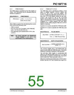
EQUATION 8-1:
PWM PERIOD
PWM Period = [(PR2) + 1] • 4 • TOSC •
(TMR2 Prescale Value)
When TMR2 is equal to PR2, the following three events
occur on the next increment cycle:
Equation 8-2 is used to calculate the PWM pulse width.
• TMR2 is cleared
Equation 8-3 is used to calculate the PWM duty cycle
ratio.
• The CCP1 pin is set. (Exception: If the PWM duty
cycle = 0%, the pin will not be set.)
• The PWM duty cycle is latched from CCPR1L into
CCPR1H.
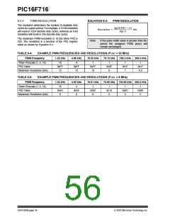
EQUATION 8-2:
PULSE WIDTH
Pulse Width = (CCPR1L:CCP1CON<5:4>) •
TOSC • (TMR2 Prescale Value)
Note:
The Timer2 postscaler (see Section 6.0
“Timer2 Module”) is not used in the
determination of the PWM frequency.
EQUATION 8-3:
DUTY CYCLE RATIO
(CCPR1L:CCP1CON<5:4>)
Duty Cycle Ratio = -----------------------------------------------------------------------
4(PR2 + 1)
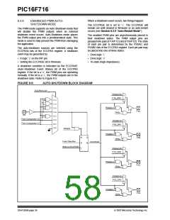
The CCPR1H register and a 2-bit internal latch are
used to double buffer the PWM duty cycle. This double
buffering is essential for glitchless PWM operation.
The 8-bit timer TMR2 register is concatenated with
either the 2-bit internal system clock (FOSC), or 2 bits of
the prescaler, to create the 10-bit time base. The system
clock is used if the Timer2 prescaler is set to 1:1.
When the 10-bit time base matches the CCPR1H and 2-
bit latch, then the CCP1 pin is cleared (see Figure 8-3).
© 2007 Microchip Technology Inc.
DS41206B-page 53

 MICROCHIP [ MICROCHIP ]