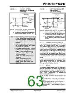
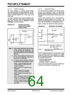
PIC16F/LF1946/47
5.2.2.6
32 MHz Internal Oscillator
Frequency Selection
5.2.2.7
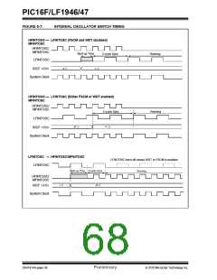
Internal Oscillator Clock Switch
Timing
The Internal Oscillator Block can be used with the 4X
PLL associated with the External Oscillator Block to
produce a 32 MHz internal system clock source. The
following settings are required to use the 32 MHz inter-
nal clock source:
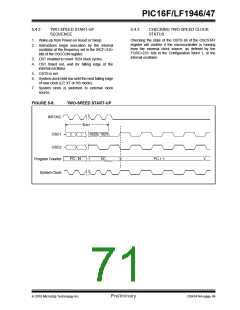
When switching between the HFINTOSC, MFINTOSC
and the LFINTOSC, the new oscillator may already be
shut down to save power (see Figure 5-7). If this is the
case, there is a delay after the IRCF<3:0> bits of the
OSCCON register are modified before the frequency
selection takes place. The OSCSTAT register will
reflect the current active status of the HFINTOSC,
MFINTOSC and LFINTOSC oscillators. The sequence
of a frequency selection is as follows:
• The FOSC bits in Configuration Word 1 must be
set to use the INTOSC source as the device sys-
tem clock (FOSC<2:0> = 100).
• The IRCF bits in the OSCCON register must be
set to the 8 MHz HFINTOSC selection
(IRCF<3:0> = 1110).
1. IRCF<3:0> bits of the OSCCON register are
modified.
2. If the new clock is shut down, a clock start-up
delay is started.
• The SPLLEN bit in the OSCCON register must be
set to enable the 4xPLL, or the PLLEN bit of the
Configuration Word 2 must be programmed to a
‘1’.
3. Clock switch circuitry waits for a falling edge of
the current clock.
4. The current clock is held low and the clock
switch circuitry waits for a rising edge in the new
clock.
Note:
When using the PLLEN bit of the
Configuration Word 2, the 4xPLL cannot
be disabled by software and the 8 MHz
HFINTOSC option will no longer be
available.
5. The new clock is now active.
6. The OSCSTAT register is updated as required.
7. Clock switch is complete.
The 4xPLL is not available for use with the internal
oscillator when the SCS bits of the OSCCON register
are set to ‘1x’. The SCS bits must be set to ‘00’ to use
the 4xPLL with the internal oscillator.
See Figure 5-7 for more details.
If the internal oscillator speed is switched between two
clocks of the same source, there is no start-up delay
before the new frequency is selected. Clock switching
time delays are shown in Table 5-1.
Start-up delay specifications are located in the
oscillator tables of Section 29.0 “Electrical
Specifications”.
2010 Microchip Technology Inc.
Preliminary
DS41414A-page 65

 MICROCHIP [ MICROCHIP ]