PIC16F/LF1946/47
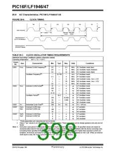
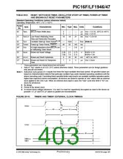
TABLE 29-2: OSCILLATOR PARAMETERS
Standard Operating Conditions (unless otherwise stated)
Operating Temperature
-40°C TA +125°C
Param
Sym.
No.
Freq.
Tolerance
Characteristic
Min. Typ† Max. Units
Conditions
OS08
HFOSC
Internal Calibrated HFINTOSC
Frequency
2%
2.5
5%
2%
2.5%
5%
—
—
—
—
—
—
—
—
16.0
16.0
16.0
500
500
500
5
—
—
—
—
—
—
8
MHz 0°C TA +60°C, VDD 2.5V
MHz 60°C TA +85°C, VDD 2.5V
MHz -40°C TA +125°C
kHz 0°C TA +60°C, VDD 2.5V
kHz 60°C TA +85°C, VDD 2.5V
kHz -40°C TA +125°C
s
(2)
OS08A MFOSC
Internal Calibrated MFINTOSC
(2)
Frequency
OS10* TIOSC ST HFINTOSC
Wake-up from Sleep Start-up Time
MFINTOSC
Wake-up from Sleep Start-up Time
—
—
20
30
s
*
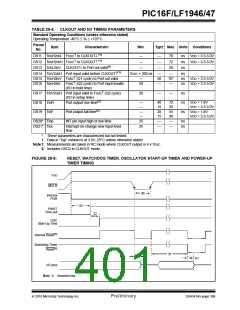
These parameters are characterized but not tested.
†
Data in “Typ” column is at 3.0V, 25°C unless otherwise stated. These parameters are for design guidance only and are
not tested.
Note 1: Instruction cycle period (TCY) equals four times the input oscillator time base period. All specified values are based on
characterization data for that particular oscillator type under standard operating conditions with the device executing
code. Exceeding these specified limits may result in an unstable oscillator operation and/or higher than expected current
consumption. All devices are tested to operate at “min” values with an external clock applied to the OSC1 pin. When an
external clock input is used, the “max” cycle time limit is “DC” (no clock) for all devices.
2: To ensure these oscillator frequency tolerances, VDD and VSS must be capacitively decoupled as close to the device as
possible. 0.1 F and 0.01 F values in parallel are recommended.
3: By design.
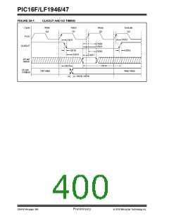
TABLE 29-3: PLL CLOCK TIMING SPECIFICATIONS (VDD = 2.7V TO 5.5V)
Param
Sym.
Characteristic
Min.
Typ†
Max.
Units Conditions
No.
F10
FOSC Oscillator Frequency Range
4
16
—
—
—
—
8
32
MHz
MHz
ms
F11
FSYS On-Chip VCO System Frequency
F12
F13*
TRC
PLL Start-up Time (Lock Time)
—
2
CLK CLKOUT Stability (Jitter)
-0.25%
+0.25%
%
*
These parameters are characterized but not tested.
†
Data in “Typ” column is at 5V, 25C unless otherwise stated. These parameters are for design guidance
only and are not tested.
2010 Microchip Technology Inc.
Preliminary
DS41414A-page 397

 MICROCHIP [ MICROCHIP ]